


OFC 2026 - High-Speed Optical Modulators for Intra-Data Center Links: Unlocking 400 Gb/s per Lane and Beyond - OFC Panel
Updated: Oct 7
Introduction
Driven by the enormous compute demands of AI training and inference (such as successive generations of large language models like ChatGPT), data center networks face extreme bandwidth challenges in both scale-out and scale-up. The latest switch ASICs already run at 200 Gb/s per lane, and the industry is now focused on the 400 Gb/s-per-lane generation expected to deploy in 2028. At OFC 2026, transmitter technologies for intensity-modulation direct-detection (IM-DD) formats took center stage. This heavyweight panel brought together technical leaders from TSMC, OpenLight, AMF, Polariton, Lumentum and Kyushu University to debate whether pure silicon photonics (SiPh) has reached its physical limits, and the brutal competition among heterogeneous materials such as InP, plasmonics, polymers and thin-film lithium niobate (TFLN) on power, bandwidth density and high-volume manufacturability (HVM).


Deep dive into core technologies and data: every company's view on record
TSMC (Sheng Kai Yeh) - Silicon microring modulators (MRM) and advanced packaging
Core technology: focuses on silicon microring modulators (MRMs), using the plasma dispersion effect of a PN junction to modulate light intensity.
Advantages and data: MRMs are wavelength-selective, offering excellent packaging compactness and high bandwidth density.
Pain points and solutions: MRMs are extremely sensitive to package temperature and process variation. TSMC's measured samples show that the maximum heater power needed to align the peak wavelength with the target wavelength is below 150 mW.
Packaging path: emphasizes 3D IC packaging integration (such as CoWoS and 3DFabric), which shortens electrical paths to reduce noise and raises system-level processing density.
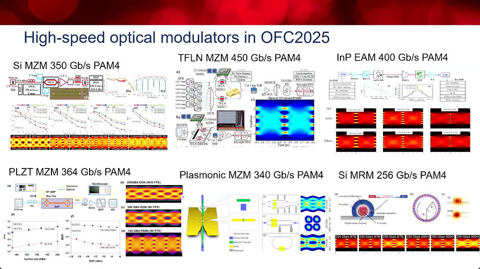


OpenLight (Beichen Wang) - Heterogeneously integrated InP EAMs on silicon photonics
Core technology: selectively integrates III-V materials heterogeneously on a standard CMOS silicon photonics platform to build electro-absorption modulators (EAMs) and integrated laser sources.
Advantages and data: excellent scalability; a single 8-inch silicon wafer can yield tens to hundreds of thousands of EAMs, sharply lowering cost and raising bandwidth density.
Performance metrics: optical insertion loss is only 1-2 dB from 10°C to 80°C. Total device length is under 400 μm, with an active modulation section under 100 μm. Measured junction capacitance is 67 fF, with 24 ohm series resistance.
Transmission results: demonstrated 400 Gb/s PAM4 transmission with a 1.8 dB extinction ratio at 2.25 Vpp drive voltage, and S21 response up to 100 GHz.


AMF (Patrick Lo) - Extending silicon photonics and a foundry strategy for new materials
Core view: continues to extend the life of silicon photonics (Mach-Zehnder and MRM) into the 200G and 400G generations through PN junction engineering.
New material integration: recognizing the physical limits of pure silicon, AMF is investing in a roadmap to integrate new materials such as thin films and polymers onto SOI base substrates.
Volume production challenges: stresses that introducing any new material (including BTO or polymers) requires, beyond reliability, compatibility with process tools, package hermeticity, and smooth integration into CMOS foundry production flows.


Polariton (Claudia Hoessbacher) - Plasmonics and organic materials
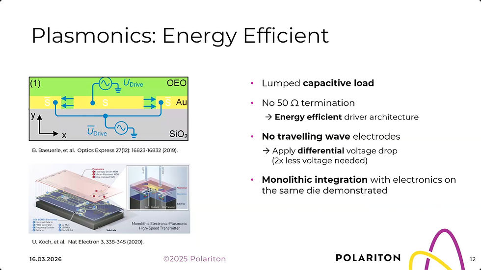
Technical breakthrough: combines metal-insulator-metal waveguides with organic electro-optic materials to break the optical diffraction limit and achieve extreme miniaturization.
Extreme specs: an active section only 15 μm long with very small capacitance, needing no 50 ohm termination, and a flat frequency response from DC to the terahertz (THz) range.
Transmission results: demonstrated 100 Gbaud (200 Gb/s) PAM4 signaling with a drive voltage of only 700 mV.
Integration potential: can be integrated by post-processing on passive components of standard silicon photonics (such as IMEC's 200 mm wafers).




Kyushu University (Shiyoshi Yokoyama) - EO polymers and perfect crystals
Core technology: develops polymers with ultra-high electro-optic (EO) coefficients and lead-free crystals (such as BTO, PZT and KNN).
Performance metrics: measurements show a clean S21 response at 81.6 GHz.
Addressing reliability concerns: responding to industry doubts about polymer stability, it showed no degradation in a 2,000-hour optical stability test at 80°C, with a glass transition temperature (Tg) of 90°C to 110°C.


Lumentum (Matthew Sysak) - InP EMLs and HVM readiness
Core advantages: InP EML devices are extremely small (tens of microns), with very high bandwidth and very low drive voltage.
Technical claim: has demonstrated network transmission at 400 Gb/s and even beyond 1.5 Tb/s (multi-lane).
Industry reality: stresses that while TFLN, BTO and polymers are very attractive on bandwidth and size, InP is currently the most commercially viable solution in terms of HVM readiness for hyperscale data centers, supply chain maturity and device robustness.


Analysis of consensus and disagreement
Consensus: co-design is absolutely necessary. All panelists agreed that in the 200 Gbaud+ generation, optical modulators cannot work alone; they need deep package-level co-design with high-speed DSPs and driver chips to solve impedance matching and excessive power.
Disagreement: ultimate performance vs. manufacturability. Foundry view: AMF and TSMC insist that no matter how innovative a material is, it cannot reach the commercial market unless it meets CMOS line process control and contamination standards, along with strict Vπ and insertion loss boundary conditions.
Emerging materials view: Polariton and Kyushu University argue that pure silicon has hit its physical limits and that plasmonics and polymers with THz potential must be boldly introduced.
The pragmatic middle ground: OpenLight and Lumentum try to balance performance and manufacturability. OpenLight brings InP's high performance onto the silicon photonics platform through heterogeneous integration, while Lumentum relies on InP's decades-old, reliable ecosystem to take on 400G directly.
Supply chain and market impact
This discussion reveals a coming shift in the tectonic plates of the optical communications supply chain. As pluggable optics evolve toward CPO (co-packaged optics) and LPO (linear pluggable optics), chip fabrication alone is no longer enough. 3D advanced packaging such as TSMC's CoWoS will become the chokepoint for optoelectronic integration. Meanwhile, if heterogeneous integration yields at companies like OpenLight keep improving, they will put strong pricing and market share pressure on traditional discrete InP laser and modulator suppliers; TFLN and polymer material suppliers, for their part, need to prove reliability and lifetime in wafer-level packaging (WLP) within the next 12-24 months.
The Simple Tech Trend view
In the 400 Gb/s-per-lane battle, pure silicon photonics (SiPh) will retreat to the role of "carrier" and "passive routing," while the heavy lifting of light emission and modulation inevitably shifts to heterogeneous materials.
Over the next 12-24 months, "silicon photonics platform + III-V heterogeneous integration" (the path OpenLight showed) will be the most investable sweet spot, combining CMOS economies of scale with InP's bandwidth performance. As for plasmonics and polymers, despite impressive 100 Gbaud+ data, solving material oxidation and CMOS line contamination concerns is the real test of whether they can cross the valley of death. The winners of the 400G single-lane era will need not only to understand optical physics, but also to command a voice in 3D advanced packaging.


Comments