


TSMC Enters the Silicon Photonics Era: Three Breakthroughs Through a Circuit Designer's Eyes (OFC 2025)
Introduction
As silicon photonics becomes the key technology behind the AI data center and high-speed interconnect revolution, TSMC — the world's largest foundry — has been quietly building a complete silicon photonics manufacturing and integration ecosystem. In this talk, TSMC shared its internal experience with design–technology co-optimization and introduced three landmark technologies, along with the new opportunities they open up for circuit designers.
📌 TSMC's Three Technical Breakthroughs
1️⃣ Silicon Photonics Process Platform
TSMC has developed a production-ready silicon photonics process node, deliberately built on mature process technology to keep cost and mask complexity down.
It ships a complete PDK covering optical couplers (grating / edge couplers), modulators (microring / Mach-Zehnder), waveguides, photodetectors, and multiplexing components.
It supports co-simulation with electronic circuits and is integrated with the major EDA vendors.

2️⃣ SoIC-X: High-Density 3D Interconnect
An ultra-short-reach, ultra-high-density die-to-die interconnect with pitch below 15 µm and thickness under 10 µm.
It has passed TSMC's volume-production qualification and targets die stacking for high-speed data transfer.
It raises interconnect density while shrinking package footprint and power.

3️⃣ COUPE (Compact Universal Photonic Engine)
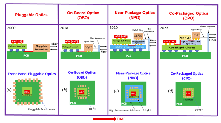
Stacks the electronic and photonic ICs vertically: an advanced CMOS node on top (e.g., N7) and the silicon photonics platform underneath (e.g., N65).
SoIC-X provides the ultra-short connection between the two, sharply reducing area and improving transmission efficiency.
The result is a low-power, high-bandwidth, highly integrated packaging solution for data centers and AI hardware.

🛠 Opportunities and Takeaways for Circuit Designers
New architectures enabled by ultra-short interconnects
Because the electrical connections are so short, termination and equalization circuits (CTLE) can be dropped.
Simulations show only 0.3 dB of loss at 100 GHz.

An inductor density revolution: vertical dual-layer and 3D inductors
A two-die design lets each die's metal stack host its own inductor, raising inductor density.
Vias and interconnect lines can form 'vertical inductors' that consume almost no horizontal area.
This is especially valuable for area-sensitive RF and optical-communication circuits such as distributed amplifiers.
Active circuit innovation
New low-noise TIAs (Cherry-Hooper architecture) and high-swing drivers (referencing an Intel design).
An active thermal tuning loop for microring modulators to compensate for process and temperature drift.
🔍 Q&A Highlights
Optical coupling: TSMC offers both grating and edge couplers. Grating couplers tolerate misalignment better but have higher loss; edge couplers offer wider bandwidth but are harder to align.
Capacitance: One academic noted that short-reach interconnects cut capacitance to as low as 6–7 fF, which lowers power and reduces the laser power required.
Vertical inductors: Built from TSMC's interconnect stack and vias, they deliver practical inductance in the hundreds of pH for high-speed applications.
Conclusion
With three innovations — its silicon photonics process, SoIC-X interconnect, and COUPE integrated packaging — TSMC is building the next-generation optoelectronic integration platform. As these technologies mature, they bring not only a breakthrough in high-speed transmission but a new horizon for analog design and 3D packaging. For circuit designers, this is not just a process upgrade; it is a major expansion of design freedom.


Comments