


ECOC 2026 | Technical Analysis | NVIDIA Aligns Nine Microrings to Nine Lasers: In a 2.78 pJ/b DWDM Optical Link, the Hard Part Isn't Speed, It's "Boot-Up"
NVIDIA's ECOC 2026 paper doesn't solve a speed problem. It solves a boot-up problem. Earlier this year at ISSCC and OFC, they presented a microring DWDM test chip — 256 Gb/s per fiber, 2.78 pJ/b, and 0.8 Tb/s/mm shoreline density. Beautiful numbers. But behind that beautiful eye diagram, nine TX microrings and nine RX microrings each have to align to nine lasers, and the chip can't see the spectrum, doesn't know where the lasers are, and doesn't know its own absolute wavelength. In the lab you can tune by hand; in a product you can't. This paper delivers the automated solution: Static Ring Assignment (SRA) finds the ring-to-laser mapping with the lowest total heater power at boot-up; Dynamic Ring Assignment (DRA), as the chip temperature drifts, rotates the entire mapping while data keeps flowing — including moving the forwarded clock from one channel to another without dropping a single bit.
1. Paper Background: Who Published It and Why It Matters
Affiliation: NVIDIA Corporation (teams in Santa Clara, Durham, and Ridgefield)
Conference: 2026 European Conference on Optical Communication (ECOC 2026), September 22, 2026
Presenter: Angad S. Rekhi
Co-authors: Stephen G. Tell, Brian Zimmer, Li Xu, Georgios Kalogerakis, Sanquan Song, Nandish Mehta, Nikola Nedovic, Yoshi Nishi, Xi Chen, Ward Lopes, Benjamin G. Lee, Thomas H. Greer III, C. Thomas Gray
Why does it matter? Because this isn't another "we built a faster optical link" paper. It's a paper about handing the physics of optical components over to digital control loops to tame — and that is exactly the threshold microring DWDM must cross to go from paper to product.
Microrings are small and many can be cascaded on a single bus, making them the most direct path to higher shoreline density. Their downside is just as simple: a microring's resonant wavelength is extremely temperature-sensitive. Shift the chip temperature by a few degrees and the resonance walks off. To keep it working, every ring needs a heater and a closed loop.
With one ring, that's a control problem. With eighteen rings (nine TX, nine RX) each locking onto nine lasers, it becomes a combinatorial optimization problem.

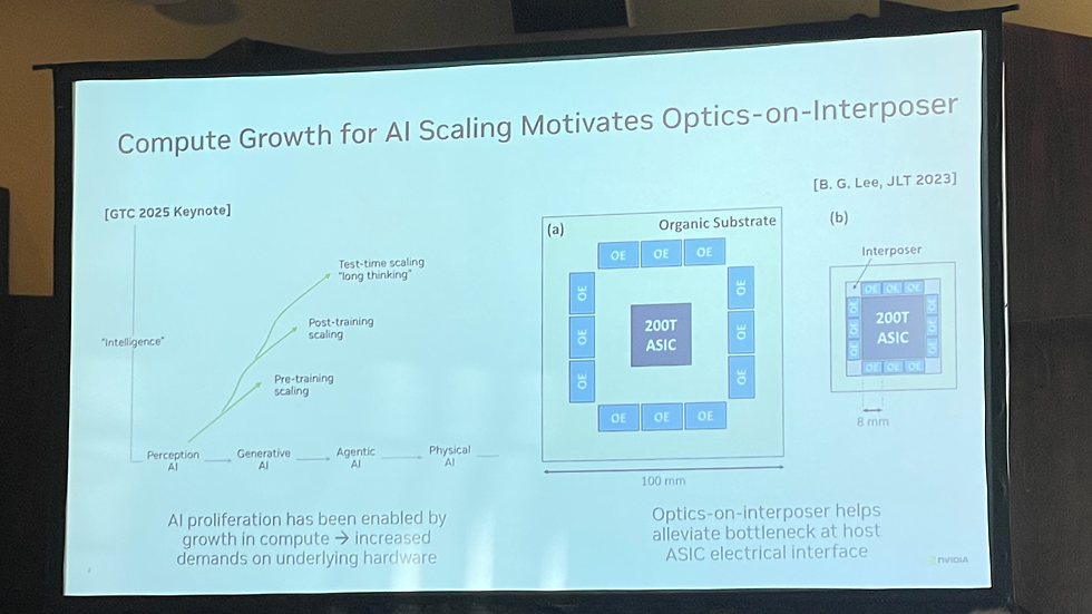
2. Why Optics-on-Interposer: 100 mm Shrinks to 8 mm
The first content slide states the motivation bluntly, with a very visual comparison.
What the slide shows: the left half is the "intelligence growth" curve from the GTC 2025 keynote — perception AI → generative AI → agentic AI → physical AI — overlaid with three acceleration curves: pre-training scaling, post-training scaling, and test-time scaling ("long thinking"). The right half is an architecture comparison cited from B. G. Lee, JLT 2023.
Key numbers / findings: panels (a) and (b) on the right are the point. Take the same 200T ASIC:
(a) On an organic substrate, optical engines (OEs) surround the ASIC and the substrate is 100 mm wide
(b) On an interposer, the optical engines sit right next to the ASIC, just 8 mm away
Industry implications: going from 100 mm to 8 mm isn't "better" — it's an order-of-magnitude-plus difference in electrical trace length. Trace length directly sets how strong a SerDes you need, how big a DSP, and how much power. That is the entire argument for optics-on-interposer — bypass the host ASIC's electrical-interface bottleneck altogether.
The other half of this route — the laser array — we covered in ECTC 2026 | NVIDIA | Light Shouldn't Be Forced into Electrons and Back: Why NVIDIA's DWDM Laser Array Rewrites the Economics of Optical Interconnect.
3. The Test Chip: Where 2.78 pJ/b and 0.8 Tb/s/mm Come From
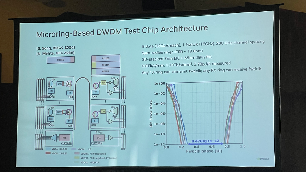
What the slide shows: the full architecture and specs of the test chip, citing S. Song (ISSCC 2026) and N. Mehta (OFC 2026). On the left, the circuit block diagram (TX0…TX8, RX0…RX8, and the CLKCMN shared clock block); on the right, the BER-vs-forwarded-clock-phase bathtub curve.
Key numbers / findings:
8 data channels at 32 Gb/s each; 1 forwarded clock (fwdclk) at 16 GHz — i.e., a half-rate clock
200 GHz channel spacing
5 µm radius microrings, FSR ≈ 13.6 nm
3D stacking: 7 nm EIC + 65 nm silicon photonics PIC
Measured 0.8 Tb/s/mm, 1.33 Tb/s/mm², 2.78 pJ/b
Any TX channel can send the forwarded clock; any RX channel can receive it
Bathtub curve: 0.47 UI eye opening at a 1e-12 error rate
8 × 32 Gb/s = 256 Gb/s per fiber.
Industry implications: three things. First, a shoreline density of 0.8 Tb/s/mm sits well above the "more than 0.3 T/mm" target Huawei set for a 1024-lane switch at the same conference — microring DWDM really can push density. Second, 2.78 pJ/b is already below 3, and that's a full link including the clock. Third, and easiest to miss — the design choice that "any channel can send or receive the clock" isn't flexibility for its own sake; it's the premise of the entire second half of the paper.

4. The Core Problem: The Chip Is Blind
What the slide shows: the problem definition for Static Ring Assignment (SRA). On the left, a through-port spectrum, wavelength 1290–1310 nm on the x-axis and through power in dBm on the y-axis; the dashed lines are the nine laser wavelengths, λ0 (reddest) to λ8 (bluest), and the green arrows show how far each ring must be heated. Top right is a "roulette wheel" diagram: the outer ring shows ring resonance positions, the inner ring the laser wavelengths.
Key numbers / findings: the presenter stressed an important point — this spectrum is only for illustration; the chip itself has no way to observe the spectrum directly.
The full problem statement: with no access to the lasers, no access to the fiber connection, and no knowledge of absolute wavelength, use only on-chip resources to find the power-optimal ring-to-laser mapping.
There are two constraints:
Spectral order must equal spatial order (the rings' physical order on the bus), because this reduces crosstalk
But the whole mapping may rotate once around the FSR — and that is the key to saving power
Industry implications: the second constraint is the paper's cleverest move. There is always a process offset between the ring grid and the laser grid. If you force "ring 0 must pair with laser 0," some rings must be heated a lot to get into place. But if the whole mapping is allowed to rotate — e.g., ring 4 to λ0, ring 5 to λ1, … ring 0 to λ5 — total heater power can drop dramatically.
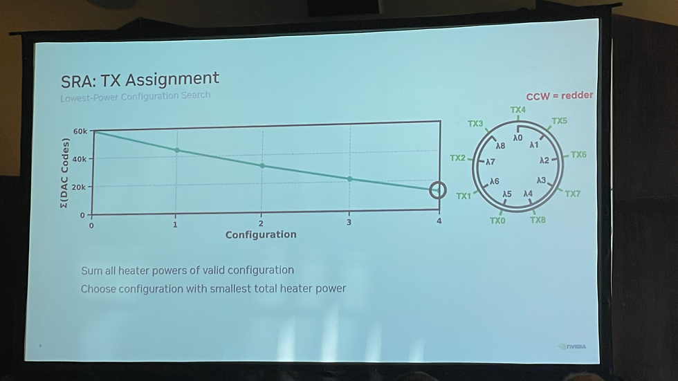
The roulette-wheel design itself is worth learning from: the outer ring is continuous (because a ring's resonance repeats every FSR), while the inner ring is broken (because laser wavelengths have no such periodicity). Counter-clockwise is redward; clockwise is blueward.

5. All the Chip Can See Are Two Numbers: ADC Code and DAC Code
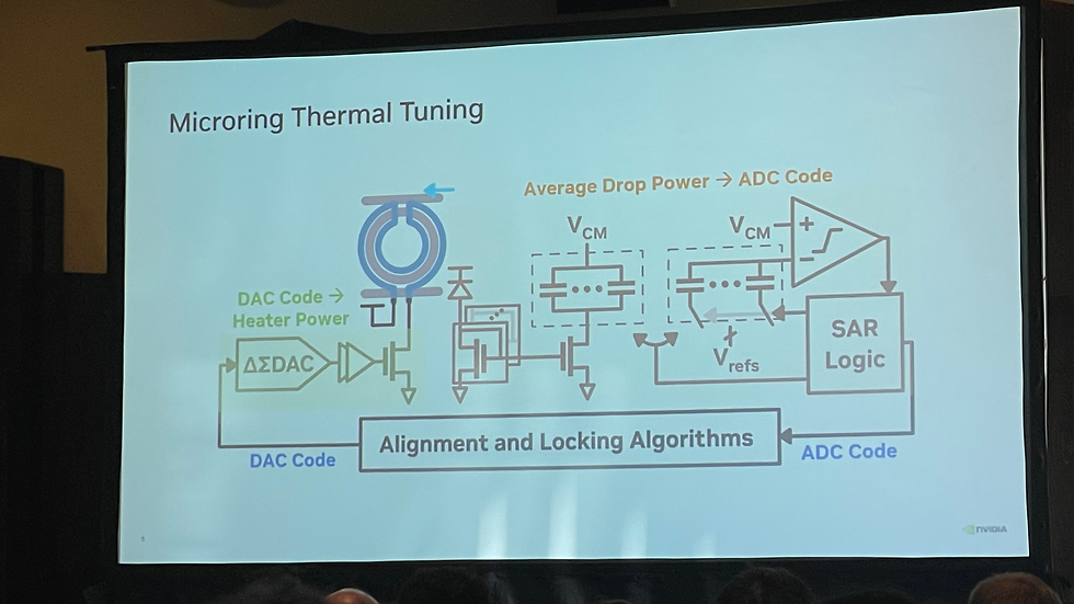
What the slide shows: the full microring thermal-tuning loop. On the left, the ring and its heater, driven by a ΔΣ DAC; on the right, the drop port's average optical power digitized via SAR logic into an ADC code; bottom center, the "alignment and locking algorithm" block.
Key numbers / findings: you only need to remember two mappings for the whole paper:
ADC code ≈ average drop-port optical power (the chip's "eyes")
DAC code ≈ heater power (the chip's "hands")
Industry implications: this slide is the whole design philosophy in miniature. The chip has no spectrometer — just one ADC and one DAC. All the intelligence has to grow out of one thing: sweep the DAC code and watch how the ADC code changes. That's also why this approach can go into a product — it needs no external measurement equipment.
6. SRA on the TX Side: From One Sweep to One Minimal Rule
What these slides show: the TX-bus static assignment flow, ring by ring. The x-axis is DAC code 0 to 8192; the y-axis is ADC code.
Step one: sweep the first ring on the bus, TX0, from hot to cold (DAC code high to low) and record drop-port power. Lasers appear as peaks on the sweep curve. There's a very honest observation here: without self-heating, the peaks would be neat Lorentzian lineshapes; what's actually measured are sharp triangles — meaning self-heating is significant on this chip.
Step two: pick a laser to lock onto. The example picks the one with the "second-highest heater power" (λ2). The locking method: first heat the ring past that laser so it enters the correct hysteresis state, then lock back to the point at about 75% of the measured peak drop power — the OMA-optimal position.
Step three: repeat the sweep for each subsequent ring and use peak prominence to tell lasers already taken by upstream rings from lasers still free. For example, when TX1 sweeps across λ2, its power is clearly lower than the other lasers it sees, because λ2 has already been locked by upstream TX0 — this is called a captured laser.
Then comes the minimal rule:
The target ring being assigned should lock to the first uncaptured laser it sees after the last captured laser.
With a hot-to-cold sweep direction, this rule automatically guarantees that the target ring locks to the reddest uncaptured laser, and that spectral order equals spatial order, allowing one rotation around the FSR. If a ring sees no captured laser at all, it locks to the one requiring the highest heater power.
Step four: once every ring is assigned, the configuration is called a valid configuration, and its total heater power is summed. Then TX0 is re-locked to the laser with the "next-lowest heater power" and the process reruns, enumerating the options. The configuration with the lowest total heater power is the final choice.
Industry implications: the elegance of this flow is that it reduces a global optimization problem to a local per-ring rule plus a bounded enumeration. And assigned rings stay closed-loop locked throughout, unaffected by later steps. The presenter also candidly noted more corner cases (e.g., a ring seeing two consecutive groups of captured lasers), which are left to the paper.


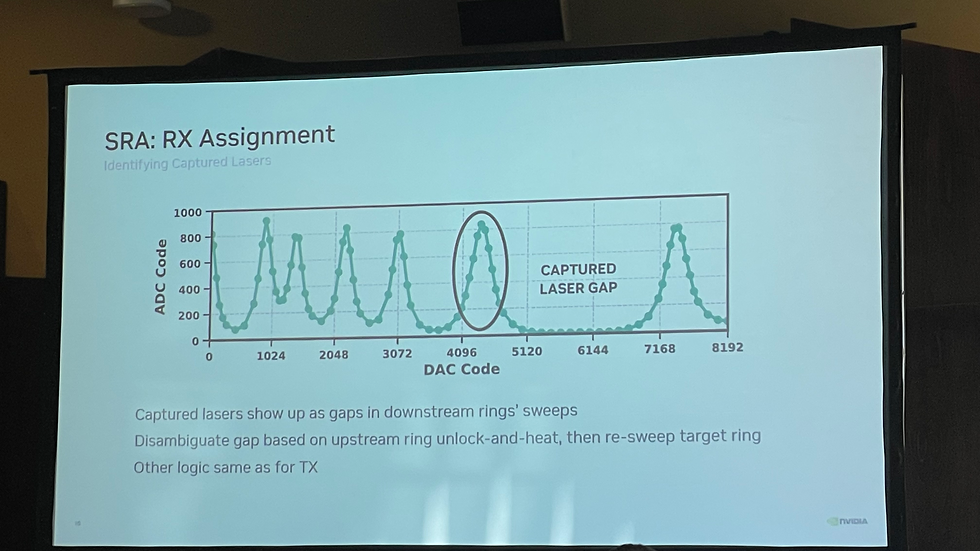
7. SRA on the RX Side: Captured Lasers "Disappear"
What the slide shows: the sweep curve during RX-bus assignment, again DAC code 0 to 8192 on the x-axis and ADC code 0 to 1000 on the y-axis. A region labeled CAPTURED LASER GAP is circled on the plot.
Key numbers / findings: the RX side has a headache the TX side doesn't. Because RX rings lock on resonance, rather than off resonance as TX rings do, a laser captured by an upstream RX ring doesn't show up at all in the downstream ring's heater sweep — it doesn't get weaker, it vanishes entirely.
So the logic has to be inverted: look for gaps between uncaptured lasers, and treat a gap as evidence of a captured laser.
But a gap can come from three sources: a genuinely captured laser, an FSR gap that happens to fall in the ring's spectrum, or variation in the laser line spacing. How to tell them apart? The paper's method is direct:
Unlock the immediately upstream ring, heat it slightly, and re-sweep the target ring. If a new laser appears, the gap is a "capture gap." Once confirmed, the upstream ring is re-locked correctly, and the target ring is locked to the laser at a slightly lower DAC code relative to the capture gap.
Industry implications: this "unlock upstream, heat, re-sweep" trick isn't just for RX. The presenter added a very practical note — if laser power is uneven enough that a simple power threshold can't distinguish captured from uncaptured lasers on the TX side, the TX side can use the same procedure too. In other words, the design is robust to laser power non-uniformity.
8. DRA: Rotating the Mapping While Data Runs
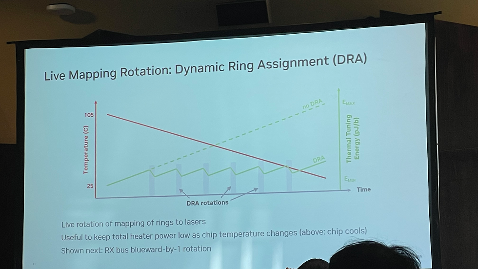
What the slide shows: the motivation for Dynamic Ring Assignment (DRA). The x-axis is time, the left y-axis chip temperature (falling from 105°C to 25°C), the right y-axis thermal-tuning energy (pJ/b). The red line is temperature, the green line thermal-tuning energy — dashed is "without DRA," solid is "with DRA"; the solid line is sawtoothed, and each drop is labeled "DRA rotation."
Key numbers / findings: the chip cools from 105°C to 25°C, an 80°C temperature range. Without DRA, keeping every ring's resonance in place requires ever more heater compensation, so thermal-tuning energy rises monotonically. But if the ring-to-laser mapping is allowed to rotate live, total heater power can stay relatively low across the entire temperature range.
Industry implications: this matters especially for CPO / optical engine builders. The most common objection to microring DWDM is thermal-tuning power — you save DSP power only to spend it on heaters, so is it worth it? This slide's answer: if your control logic is smart enough, thermal-tuning power doesn't have to climb monotonically with temperature drift. That downgrades the "microrings aren't practical" objection from a physics problem to a control problem.
9. The Cost of Rotation, and the Clock Swap That Costs Nothing
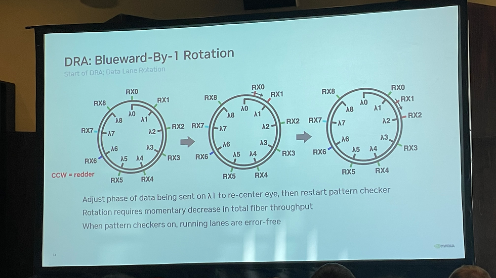
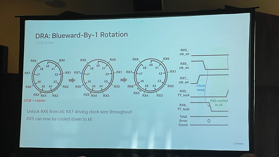
What these slides show: the full process of a blueward-by-1 rotation on the RX bus, shown as a sequence of roulette-wheel diagrams, with timing diagrams in the last few. Green means the channel is receiving data, blue means it's receiving the clock, red means that channel's pattern checker is stopped. Dark blue means the received clock is driving the clock line used to sample data; light blue means it isn't driving anything yet.
Rotating data channels is simple: stop the pattern checkers on two channels, unlock two rings, freeze the heater codes; move RX0 clockwise (blueward) to λ1 and lock it; adjust the phase of the data sent on that wavelength to re-center the eye, then restart the pattern checker. The slide says it plainly: rotation requires a brief dip in total fiber throughput, but the remaining channels are error-free while their pattern checkers are running.
The clock-channel swap is where the paper truly shines. The scenario: RX4 has just taken λ5, RX5 is unlocked and frozen, ready to cool to λ6. But to do that, RX6 must first be unlocked — and RX6 is receiving the very clock that drives the clock line. Unlock it and the whole link goes down.
The solution: first, have the clock received by RX7 also start driving the same clock line. During this period, RX6 and RX7 drive the same clock line simultaneously, without a single bit error.
Second, unlock RX6 from λ6. Because RX7 has already taken over driving the clock line, this step is also bit-error-free. Third, this frees up room so RX5 can cool to λ6 and the rotation continues.
The bottom-right column of the timing diagram reads Total Error Count: 0.
The presenter added: this swap works not only when two RX channels share the same clock line; they also verified functional operation with two RX clock channels driving different clock lines, again with no bit errors.
Industry implications: the power benefit of clock forwarding is clear — the receiver needs no CDR. But it has always had a structural weak point: the clock channel is a single point of failure, and it can't be moved. This paper proves that the clock channel can be thermally migrated too, with the link live and zero bit errors. That turns clock forwarding from "power-efficient but rigid" into "power-efficient and reschedulable."


10. Technical Highlights: Two "Impossibles" Solved
Boil the paper down and there are two real innovations — and neither is at the device level.
First, "allowing rotation" turns combinatorial explosion into a power-saving degree of freedom. Nine rings to nine lasers, rigidly one-to-one, is an inflexible constraint; allow the whole set to rotate around the FSR and you get nine equivalent configurations whose total heater power can differ widely. The paper turns a physical phenomenon that was a "limitation" (FSR periodicity) into an optimization search space.
Second, the hot swap of the forwarded clock. This is the part I think deserves to be remembered most. In a system where the clock must stay valid at all times, moving the clock source from one channel to another without dropping a bit — that's not easy even in the electrical world, and in optics you add thermal-tuning hysteresis and lock time on top. They solved it with a seemingly plain trick: "two channels briefly drive the same line at the same time."

11. Industry Connection: How Far Is This from Volume Production?
To be honest: this is a test chip, not a product. But the nature of this paper defines its place — it tackles exactly the stretch between "test chip" and "product."
The presenter made this clear at the outset: "Measuring these bathtub curves in the lab is one thing, but doing it in a product requires a robust, automatic, and repeatable solution." Those three adjectives are the paper's entire purpose.
The microring DWDM route is now being pushed by NVIDIA and by the OCI camp of Meta / Broadcom / AMD at the same time. The OCI 200G line-side spec also uses microring DWDM with external lasers, which we broke down in Technical Analysis | Meta, Broadcom, and AMD Jointly Define the OCI 200G Line-Side Spec. Everyone on this route has to solve the same boot-up problem.
12. Conclusion
Here's where I think this paper sits in technical history: for the past decade, microring DWDM has been treated as "the densest in theory, too hard to control in practice." This paper breaks down what "too hard to control" actually means, then solves it item by item.
For Taiwan's supply chain, three concrete takeaways:
First, remember the 0.8 Tb/s/mm figure. It's more than double the 0.3 T/mm target Huawei set for a 1024-lane switch at the same conference. Microring DWDM isn't the only route that can hit the target, but it's the one that has put its numbers on the table along with a complete control scheme. For Taiwanese companies doing optical engine packaging, FAUs, and high-density optical interfaces, this means the microring route's volume-production timeline shouldn't be underestimated.
Second, the answer to the thermal-tuning power debate has changed. The core argument against microrings used to be "the heaters eat back the power you saved." DRA's 105°C-to-25°C chart responds: not if the control logic allows the mapping to rotate. For anyone weighing microrings against other modulator routes (EAM, TFLN, BTO), this is an input that needs recalibrating.
Third, and most easily overlooked — this paper's value is in the "software." SRA and DRA are algorithms, not new materials or new processes. That means part of this route's competitive moat will lie in digital control-loop design capability, not just optical process. For Taiwanese companies, that's both bad news (it's not our traditional strength) and good news (it requires no new fab investment).
Verdict: this paper's biggest contribution isn't the 2.78 pJ/b — it's proving that microring DWDM's "uncontrollability" can be solved in code. When nine rings can find nine lasers on their own on a blind chip, and re-shuffle while carrying data through an 80-degree temperature drift, microrings stop being a technology that needs someone standing beside it. That is the watershed for whether it makes it into products.
This article is for technology and industry trend analysis only and does not constitute investment advice.
References
Angad S. Rekhi, Stephen G. Tell, Brian Zimmer, Li Xu, Georgios Kalogerakis, Sanquan Song, Nandish Mehta, Nikola Nedovic, Yoshi Nishi, Xi Chen, Ward Lopes, Benjamin G. Lee, Thomas H. Greer III, C. Thomas Gray, "Static and Dynamic Ring Assignment in a Clock-Forwarded DWDM Optical Link," 2026 European Conference on Optical Communication (ECOC 2026), September 22, 2026. NVIDIA Corporation (Santa Clara, CA / Durham, NC / Ridgefield, CT, USA)
B. G. Lee et al., "Beyond CPO: A Motivation and Approach for Bringing Optics Onto the Silicon Interposer," Journal of Lightwave Technology (JLT), 2023.
S. Song et al., "A 32 Gb/s/λ 256 Gb/s/Fiber Half-Rate Bandpass-Filtered Clock-Forwarding DWDM Optical Link in a 3D-Stacked 7nm EIC/65nm PIC Technology," ISSCC 2026.
N. Mehta et al., "A 256 Gb/s DWDM Optical I/O in a 3D-stacked EIC/PIC Silicon Photonics Platform," OFC 2026.
Related Reading
ECTC 2026 | NVIDIA | Light Shouldn't Be Forced into Electrons and Back: Why NVIDIA's DWDM Laser Array Rewrites the Economics of Optical Interconnect: the laser side of the same route — NVIDIA and Lumentum's production-grade DWDM laser array
Technical Analysis | Meta, Broadcom, and AMD Jointly Define the OCI 200G Line-Side Spec: A Scale-Up Bet on Single-Fiber Bidirectional, Microring DWDM, and External Lasers: another camp betting on microring DWDM, and the specs it draws up for external lasers


Comments