


The Great Shift in Photonics Packaging (Part 1): From Back-End Assembly to Value Core — Why This $14B Market Suddenly Got Hot
For the past decade, almost no one in the industry voluntarily brought up "photonics packaging." It was filed under the last mile of OT (optical transceiver) module assembly — its value taken for granted, with little difference in who did it. Then AI pushed the power consumption of scale-up and scale-out interconnect to the limit, and packaging suddenly jumped from backstage to center stage.
Combining multiple industry estimates, the global photonics packaging market will grow from about $4.5B in 2025 to $14.4B in 2031, a CAGR of about 21.4%. This isn't the transceiver business itself exploding — pluggable optical transceivers grow at only about 10% CAGR over the same period, from $4.4B to $7.8B. The real increment comes from three new tracks opening at once: CPO from $0.1B to $5.1B, AR display engines from $20M to $1.4B, and FMCW LiDAR from zero to $172M.
What these three tracks share isn't the "optical communications" label but this: packaging is shifting from a back-end optimization to a front-end design constraint. Whoever defines the new rules gets the next round of rewards.
1. Why Now: AI Has Pushed Packaging from Backstage to Center Stage
In 2025, global hyperscaler capital expenditure surged to about $445B. Where is that money going? The four leaders — Microsoft, Google, Meta and Amazon — account for about $330B, all poured into next-generation data centers. Once compute is stacked up, the problem returns to the familiar place: interconnect power.
The promise of optical interconnect has never changed — bring light closer to the logic, trade wavelengths for power, and reduce the cost of SerDes. The question is "how close." Over the past decade, pluggable optics put the light on the faceplate and relied on copper traces back to the ASIC; OBO (on-board optics) and NPO (near-packaged optics) tried to bring light onto the motherboard or even next to the ASIC, but neither took off, and most stayed at proof-of-concept.
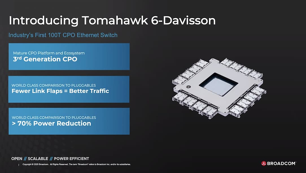
The real turning point was 2025: NVIDIA unveiled its Spectrum-X Photonics CPO switch at GTC, Broadcom's Tomahawk-series CPO entered testing at Meta, Intel showed a 4 Tbps optical I/O chiplet co-packaged on a CPU, and TSMC formally positioned COUPE as a production-ready platform. This isn't one company sloganeering — the whole ecosystem declared at once that "light really is moving next to the ASIC."

When the optical path shrinks to inside the ASIC package, packaging is no longer just "assembling the module." It becomes:
Alignment accuracy requirements entering the sub-micron range
Managing optical, electrical, thermal and mechanical interfaces simultaneously
No fixing it after tape-out — the packaging strategy must be decided at the chip design stage
A PIC isn't really finished until its packaging strategy is settled.
That sounds like philosophy, but it's engineering reality. Grating coupler placement, edge coupler facets, I/O pad locations, thermal island distribution — if these aren't decided at the layout stage, what follows is a redesign or a yield collapse.
2. Three New Tracks: CPO, AR microLED, FMCW LiDAR
Breaking down the overall $14.4B market, the 2031 structure looks like this:
Application | 2025 Size | 2031 Size | 6-Year CAGR |
Pluggable Optical Transceiver | $4.4B | $7.8B | ~10% |
CPO (incl. OBO/NPO/scale-out/scale-up) | $0.1B | $5.1B | ~92% |
AR Display Engine | $20M | $1.4B | ~102% |
FMCW LiDAR | 0 | $172M | – |
Total | $4.5B | $14.4B | ~21.4% |
Track one: CPO elevates packaging from "assembly" to "advanced packaging." At its core, CPO stacks the PIC and EIC, which requires hybrid bonding or fan-out micro-bump technology — the territory of pure-play foundries and high-end OSATs. The market-share leaders of the pluggable era — Fabrinet, Jabil, Luxshare, Innolight and Eoptolink — will lose home-field advantage in this transition, and value will shift toward players with advanced packaging capabilities such as TSMC, ASE and SPIL.
Track two: AR microLED pulls packaging into display applications. This is the most overlooked track. While everyone talks about Meta Ray-Ban Display and Google × Magic Leap AR glasses, the real underlying bottleneck is "how to bond the epi-wafer to the CMOS backplane." This hybridization step doesn't count as packaging in traditional display definitions, but microLED is the only display technology that requires it, so a substantial share of the entire display engine's value will land with packaging houses. Monolithic RGB microLED volume production in 2028 is the key milestone.
Track three: FMCW LiDAR pulls photonics packaging into automotive. dToF remains mainstream in the near term, but FMCW — with built-in velocity measurement, compatibility with SiPh platforms and the potential to lower sensor cost — is expected to start entering vehicles in 2028–2030. SiLC, Voyant, Scantinel (acquired by MicroVision) and Aeva are the first candidates. Automotive requirements for hermetic packaging and environmental testing are stricter than datacom, so packaging's share of total value on this track will rise to about 40% — well above datacom's 25%.
3. Microelectronics Philosophy Takes Over Photonics
Extract what these three tracks have in common, and a bigger narrative emerges:
Photonics packaging is adopting the philosophy of the microelectronics industry — standardization, PDK/ADK frameworks and a foundry-centered value chain.
Photonics used to be "every company for itself" — proprietary architectures, custom optical paths, manual alignment. That worked in the pluggable era because volumes were small, prices high and customization was a selling point. But CPO demands mass production; at the scale of hundreds of thousands to millions of optical engines, "custom" means "can't be built."
This shift is especially visible in Taiwan. The Silicon Photonics Industry Alliance, founded by SEMI in 2024, brings together more than 30 Taiwanese companies, including TSMC, ASE, Foxconn, MediaTek and Quanta. The whole ecosystem is reorganizing around the foundry — TSMC offering COUPE as a turnkey platform, ASE/SPIL handling the advanced packaging back end, and ShunSin (a Foxconn subsidiary) doing system integration. This structure replicates microelectronics' success model of the past two decades: the foundry defines the process, OSATs handle packaging, and fabless companies design within the PDK framework.
For fabless design companies, this means two things:
The packaging route must be chosen at the design stage — TSMC COUPE or ASE FOCoS? Hybrid bonding or fan-out? This choice in turn constrains the SiPh chip layout
Optical interfaces must go into the PDK — grating couplers, edge couplers and detachable fiber connectors (such as solutions from Teramount, Senko and ICON Photonics) must be defined at the chip-level layout stage
This shift is bad news for Europe's ecosystem. Europe has top-tier photonics research institutes such as imec, CSEM and Fraunhofer, and niche OSATs like Phix, SCINTIL and Bay Photonics, but lacks a photonics foundry that can handle volumes in the millions. Europe will likely keep its edge in high-end, low-volume markets such as quantum, defense and aerospace, while the home field for mass production will be in Asia — mainly Taiwan, followed by mainland China's Innolight and Eoptolink.
4. Three Signals Worth Tracking
Over the next 12–24 months, these three signals will set the pace of the whole transition:
Signal one: the first wave of CPO scale-out volume shipments. Actual 2026–2027 shipments of NVIDIA's Spectrum-X Photonics and Broadcom's Tomahawk CPO will set the tone for the market — if hyperscalers really adopt them, CPO inflation will be more aggressive than expected.
Signal two: TSMC COUPE's customer mix. COUPE is a turnkey platform, but who the customers are and how the share splits will determine the future distribution of power in the value chain. If NVIDIA, Broadcom and Marvell together take 70%, industry concentration will be even higher than CoWoS.
Signal three: the pace of Marvell × Celestial AI integration. Marvell's December 2025 acquisition of Celestial AI's Photonic Fabric platform is the strongest signal that the SiPh interposer route (the endgame architecture for scale-up) is industrializing. Integration progress will determine what scale-up CPO looks like in 2028+.
5. Conclusion: Whoever Defines the New Rules Wins
No one wanted to hear the photonics packaging story for the past decade because it sounded like "outsourced assembly." Over the next decade it will be discussed again and again, because it has become the most critical segment of the AI infrastructure value chain.
Going from $4.5B to $14.4B isn't just a market tripling — it's a redistribution of power in the value chain. Fabrinet, Jabil and Luxshare, which earned hard-won money in transceiver assembly, will keep growing, but at a slower rate than TSMC, ASE and SPIL, which handle advanced packaging; companies doing high-end niche work in Europe will survive, but the authority to define standards will move to Taiwan and US hyperscalers.


Comments