


The Great Shift in Optical Packaging (Part 2): CPO's Three-Stage Evolution — Why OBO Died, Scale-Out Moves First, and Scale-Up Is the Endgame
The term CPO (co-packaged optics) has been hyped for at least five years. Every OFC, someone says "volume production is next year," yet pluggable optics sell better every year. It took GTC 2025 for the market to accept that CPO is really coming: NVIDIA put Spectrum-X Photonics on the table, Broadcom sent Tomahawk CPO into Meta's test labs, and TSMC upgraded COUPE from a demo to production-ready.
But CPO will not "replace" pluggables. Based on industry estimates, pluggable optical transceivers will still grow to $7.8B by 2031 (CAGR ~10%), while CPO (including OBO, NPO, scale-out and scale-up) will surge from $0.1B in 2025 to $5.1B (CAGR ~92%). These are two parallel markets, not a substitution.
This article breaks down three questions: Why did OBO and NPO die? Why is scale-out CPO moving first? And why is scale-up CPO the real long-term race?
1. Two Failed Forerunners: OBO and NPO
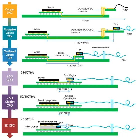
Before CPO, the industry tried two ways to "bring optics closer to the ASIC" — OBO (on-board optics) and NPO (near-packaged optics). Both died at the gate of volume production.
The core idea of OBO: move the optical module from the faceplate onto the motherboard, connected back to the switch ASIC through a socketed connector. The upside is lower faceplate power and signal loss; the downside is that both the ASIC and the PCB change, forcing a complete form-factor redesign. COBO (Consortium for On-Board Optics) was founded in 2016, Delta and Microsoft built a proof of concept in 2018, and then it stalled — hyperscalers didn't want to overhaul the entire PCB architecture for a modest power saving, and the modularity of pluggables was simply too attractive.
The core idea of NPO: move the optical engine even closer to the switch ASIC, next to the same multi-chip module, connected to an external laser module via a socketed optical connector. More aggressive than OBO, but still keeping a pluggable optical engine. Ragile Networks built samples, which never left the lab.
OBO and NPO both ended up as synonyms for "proof of concept."
They failed not because of technology, but because of timing. From 2018 to 2022, pluggables moved from 100G to 400G and then 800G, and each SerDes generation could still squeeze power down. Hyperscalers had no pain point that forced a change, so they naturally refused the form-factor and supply-chain restructuring costs OBO/NPO would bring.
What finally set CPO in motion was the 51.2T threshold. Beyond 51.2T, per-lane speed jumps from 100G to 200G, then 400G and 800G. Electrical limits become a hard bottleneck — SerDes power, PCB signal reach and faceplate beachfront density all hit their limits. At this point optics is no longer nice-to-have; it is a must-have.
2. Scale-Out Moves First: The 51.2T Inflection Point
The first application CPO captures is the scale-out network — horizontal interconnect between GPU clusters and between racks inside the data center. Why here first? Three structural reasons:
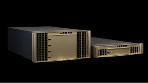
Reason 1: switch bandwidth has hit the bottleneck. From 25.6T (4 × 3.2T) all the way to 102.4T, 204.8T and 409.6T, bigger ASICs plus faster SerDes are no longer enough each generation. NVIDIA's Quantum-X800 InfiniBand reaches 115.2T with CPO in 2H 2025, and Spectrum-X will launch the SN6810 (2RU) and SN6800 (6RU) Ethernet switches in 2026–2027, targeting 409.6T.
Reason 2: scale-out topology is already stable. Spine-leaf-TOR is the standard architecture, so CPO doesn't require redesigning the cluster topology — you just swap pluggable switches for CPO switches, and the fabric logic stays the same. For hyperscalers, this is a low-risk upgrade.
Reason 3: early deployments can use 2.5D integration. The switch ASIC and optical engine (EIC + PIC) sit on the same substrate, connected through an advanced IC substrate, without needing to push to the limits of 3D hybrid bonding. This lets TSMC COUPE and ASE FOCoS ship in volume during 2025–2027.
Scale-out CPO volume is projected to rise from 39k units in 2025 to 5.97M units in 2031, a CAGR of ~131%, with revenue growing from $103M to $3.95B.
But this is just the warm-up. What will carry CPO through its second decade is scale-up.
3. Scale-Up Is the Endgame: Putting Optics Right Next to the GPU
A scale-up network is the high-bandwidth, low-latency interconnect within a single server or multi-die package — GPU to GPU, and GPU to HBM. Today this link runs on NVLink (NVIDIA), Infinity Fabric (AMD), ICI (Google TPU) and NeuronLink (Amazon Trainium 2) — all copper, using die-to-die copper traces or fly-over cables.
The problem: as clusters scale from 8 GPUs (H100) to 72 (B200), and then toward 144 or even 256, copper hits its physical limits. Each link costs 1+ pJ/bit, and with cooling on top, the bigger the cluster, the worse the economics.
Here the promise of optics is even stronger: advanced CPO architectures can reach sub-1 pJ/bit, with 30–50% system-level power savings. For hyperscalers, that is a difference measured at hyperscale.
But scale-up CPO packaging is a full level harder than scale-out:
It must go 3D-stacked: EIC on top of PIC (or vice versa), connected directly via hybrid bonding or fan-out, with signals routed through TSVs
The PIC is not just a transceiver — it becomes an interposer: the future architecture uses the PIC directly as an optical interposer between HBM and the GPU
Thermal design must be rethought: 3D stacking concentrates hot spots, and optical components are sensitive to temperature drift (laser wavelengths shift, ring resonators detune)

Scale-up CPO volume is projected to rise from 33k units in 2025 to 15.2M units in 2031, a CAGR of ~178%, with revenue growing from $30M to $3.7B.Note this 178% CAGR — it means real take-off happens in 2028, not 2026. For fabless designers and OSATs, that leaves a three-year window to prepare capacity.
4. Timeline of the Three-Stage Evolution
Laying the whole evolution out on a single timeline:
Period | Main Arena | Packaging Focus | Key Players |
2018–2025 | Pluggables dominate; OBO/NPO die as proofs of concept | Module assembly, hybrid integration | Innolight, Eoptolink, Fabrinet, Jabil, Luxshare |
2025–2027 | CPO scale-out takes off | 2.5D advanced packaging, EIC-PIC stacking | TSMC (COUPE), ASE (FOCoS), NVIDIA, Broadcom |
2027–2030 | CPO scale-up ramps | 3D hybrid bonding, heterogeneous integration of laser | TSMC, Intel (OCI), Marvell-Celestial AI, Lightmatter |
2030+ | SiPh interposer endgame | PIC as active interposer; new material platforms such as TFLN/BTO | The same group as above, joined by chiplet players such as Ayar Labs |
On the optical transceiver side, a parallel evolution is under way:
Before 2024: mainly hybrid die attach (flip-chip lasers)
2026–2028: shift to heterogeneous die attach (Intel-style wafer-level InP laser integration)
2028+: new material platforms (TFLN, BTO) enter for modulators, with heterogeneous and hybrid integration coexisting
5. NVIDIA and Broadcom Are Not Taking the Same Road
In the first wave of scale-out CPO volume production, NVIDIA's and Broadcom's architectural choices are worth dissecting, because they foreshadow how future standards will be set.
NVIDIA Quantum-X takes the 3D-stacking + TSMC COUPE route. Each optical engine has 3 PIC-EIC stacks, with EIC and PIC joined by die-to-wafer hybrid bonding using TSMC's SoIC-X. The switch ASIC and optical engines sit on the same advanced IC substrate as a multi-chip FCBGA. The modular design lets NVIDIA pair the same ASIC with different PICs, so future generations don't require rebuilding the entire architecture.
Broadcom Tomahawk CPO takes the fan-out wafer-level packaging route. Eight optical engines surround the ASIC, each with 64 TX + 64 RX channels at 100 Gb/s per channel. The SiPh chiplet uses dual-side fan-out to stack the PIC on the CMOS EIC, avoiding complex TSVs. Externally it uses a detachable 127μm-pitch optical connector, so fibers can be replaced in the field.

Two companies, two roads — mapping exactly onto the platform difference between TSMC (hybrid bonding) and ASE (fan-out).
This is no coincidence. NVIDIA and TSMC have worked together on CoWoS for years, so its CPO naturally extends TSMC's hybrid bonding route; Broadcom has deep ties with ASE/SPIL (ASE joined Broadcom's SiPh back-end packaging chain in 2023), so its CPO follows ASE's fan-out platform.
The coming standards battle for 1.6T and faster CPO is, at its core, a competition between two advanced packaging platforms: TSMC vs. ASE. That is the topic of the next article.
6. Conclusion: CPO Is an Additional Market, Not a Replacement
Back to the key point from the start: CPO is not the successor to pluggables — it is a new market. The reason is simple: pluggables remain the most cost-effective option for short-reach, lower-density applications, and sales of 800G specs like DR4/FR4/LR4 will keep growing through 2030.
What CPO really solves are the "scenarios pluggables can't":
High-density switches at 51.2T and above
Ultra-high-bandwidth interconnect inside GPU clusters
PIC-as-interposer architectures inside multi-die packages
All three share the same trait: "highly customized and locked to the ASIC roadmap." That's also why the CPO supply chain will be far more concentrated than pluggables — only a handful of players can co-design SiPh + advanced packaging with NVIDIA or Broadcom: Taiwan's TSMC, ASE and SPIL, plus Intel and Marvell in the US, and that's nearly the whole list.
CPO is a slow-start, fast-takeoff story. In 2025–2027, watch how fast scale-out runs; in 2027–2030, watch how scale-up grows; in 2030+, watch whether SiPh interposers become the new paradigm. This evolution will take a decade to play out, and each stage will reshape the power structure of optical communication packaging.


Comments