


The Great Shift in Optical Packaging (Part 3): TSMC vs. ASE vs. Intel — The Three Kingdoms of Advanced Packaging for Optics
Once CPO truly enters volume production, the next question is: who stacks the PIC and the EIC together? That job is no longer within an OSAT's traditional scope — it requires hybrid bonding or fan-out microbumps, a TSV interposer, optical alignment and electrical routing solved at the same time, and guaranteed yield at volume.
Three platforms are currently competing head to head: TSMC's COUPE (derived from CoWoS plus SoIC), ASE's FOCoS (under the VIPack CPO framework), and Intel's OCI (an extension of the EMIB/Foveros family). The three come from different positions — a pure foundry, a pure OSAT and an IDM — but all target the same market: becoming the standard platform supplier of the CPO era.
This article breaks down each company's technology choices, positioning and 2026 maturity. By the end you'll see that this race isn't about "who has the best technology" but "who locks in the standard first."
1. TSMC COUPE: The Foundry-Led Endgame of Integration
COUPE (Compact Universal Photonic Engine) is the optical engine concept TSMC first unveiled in 2021; in 2025 it was formally declared production-ready, with SoIC (System-on-Integrated-Chips) said to have reached production maturity. Its core positioning is clear: make the optical engine one of CoWoS's standard building blocks, so hyperscalers designing ASICs can choose optical I/O as naturally as they choose HBM.
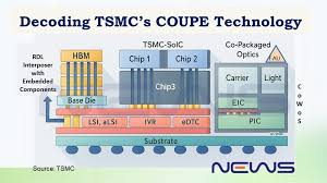
In terms of technology choices, COUPE takes the most aggressive route:
EIC and PIC connect directly Cu-Cu via hybrid bonding, no microbumps, interconnect pitch <10μm (roadmap target 3–9μm)
3D stacking, supporting both PIC-on-EIC and EIC-on-PIC
Optical coupling supports both grating couplers (GC) and edge couplers (EC); GC is friendlier to wafer-level test, EC is more efficient
Integrated within the CoWoS framework, co-built with GPUs, HBM and switch ASICs on the same silicon interposer
The price of choosing hybrid bonding: extreme requirements on wafer flatness, cleanliness and alignment accuracy. CMP must achieve atomic-level flatness, and any particle contamination makes the bond fail. That's why the technology sits with only a few players such as TSMC, Samsung and Intel — the production-line tooling and process know-how aren't something an OSAT can replicate.
COUPE isn't trying to compete with OSATs — it's trying to marginalize them in the CPO era.
Strengths: the highest bandwidth-density ceiling, the deepest co-optimization with leading-edge ASICs, and the ability to bind roadmaps directly with hyperscalers. NVIDIA's Quantum-X800 and Spectrum-X Photonics both take this route.
Weaknesses: high cost and capacity constrained by advanced-node fabs; the cycle time and capex of hybrid bonding and advanced interposers are several times those of an OSAT. CoWoS capacity is already tight, and adding COUPE won't make it easier.
2. ASE FOCoS: The OSAT's Answer for Volume
FOCoS (Fan-Out Chip on Substrate) is ASE's extension of fan-out wafer-level packaging from consumer SoCs to advanced packaging and CPO, formally under the VIPack platform. ASE joined Broadcom's SiPh back-end packaging supply chain in 2023 and announced in 2025 that CPO had entered low-volume production.

Its technology choices differ from COUPE's:
PIC and EIC connect via fan-out plus microbump / Cu pillar, interconnect pitch 20–40μm
Mainly 2D or 2.5D, with PIC and EIC side by side rather than stacked (unless the customer asks for 3D)
Signals routed through RDL (redistribution layer), with moderate overall electrical loss
No leading-edge fab process required; capacity can be expanded on existing OSAT fan-out lines
The price of choosing fan-out: larger interconnect pitch, higher parasitics, and SerDes power of about 0.5–1.0 pJ per bit (vs. 0.15–0.35 pJ for hybrid bonding). Not the first choice for applications chasing maximum density, but very friendly to mid-to-high-volume production.
Biggest strength: volume scalability and multiple OSATs able to take the work. Outside ASE, the FOCoS process can be replicated by SPIL, Amkor and Foxconn's ShunSin, which is good news for hyperscalers — it avoids single-supplier lock-in. Broadcom's Tomahawk CPO uses this route: 8 optical engines with fan-out wafer-level packaging plus dual-side attach, avoiding complex TSVs.
Biggest weakness: if CPO specs move toward extreme density (e.g. PIC-on-EIC 3D stacking becomes mainstream), FOCoS's advantage will shrink. ASE knows this; the VIPack framework already includes 2.5D enhancements such as silicon bridges, moving closer to TSMC's platform.
3. Intel OCI: The IDM's Chiplet Story
Intel's route differs from both TSMC and ASE. The core idea of Optical Compute Interconnect (OCI) is to turn optical I/O into a chiplet that can be co-packaged next to a CPU, GPU or switch — similar to UCIe, but over an optical interface.
In 2025 Intel demonstrated a 4 Tbps OCI chiplet co-packaged with a CPU — the first time an IDM truly packaged optical I/O together with logic. Its technology stack:
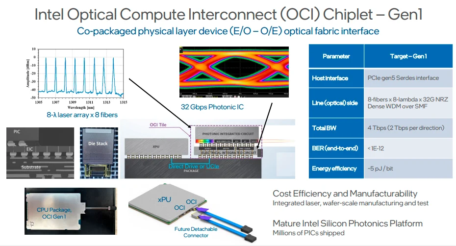
EMIB (embedded multi-die interconnect bridge) for high-density chiplet-to-chiplet connections
The Foveros family supports 3D stacking (the OCI platform currently uses mainly planar chiplet integration, but the 3D route is in place)
Optical coupling emphasizes detachable connectors, aligned with edge-style coupling, with the focus on serviceability
Leverages its own SiPh and InP laser heterogeneous integration know-how — Intel is one of the few players able to integrate InP lasers onto SiPh at wafer level
The strength of the chiplet route: a persuasive ecosystem story. OCI uses a chiplet framework aligned with UCIe, so in theory any ASIC designer adopting the UCIe standard can integrate OCI without being tied to TSMC's or ASE's packaging lines. It's a friendly option for fabless design houses.
Weakness: ecosystem maturity is still unproven. After exiting its own optical transceiver business, Intel concentrated resources on SiPh + InP heterogeneous integration, but the standardization pace of chiplet integration, and whether other ASIC vendors will adopt an Intel-style interface, are open questions. 2026 is still a pilot and limited-deployment phase, a step behind TSMC and ASE.
4. Platform Comparison Table
The key differences among the three, laid out at once:
Dimension | TSMC COUPE | ASE FOCoS (VIPack) | Intel OCI |
Lead role | Foundry-led | OSAT-led | IDM-led |
EIC / PIC connection | Cu-Cu hybrid bonding | Microbump + RDL | EMIB / Foveros |
Interconnect pitch | <10μm (roadmap 3–9μm) | 20–40μm | EMIB-class |
Integration dimension | Mainly 3D, co-built with 2.5D | Mainly 2.5D, 3D per customer | Mainly planar chiplet, 3D in place |
SerDes power | ~0.15–0.35 pJ/bit | ~0.5–1.0 pJ/bit | Depends on configuration |
Optical coupling | Both grating + edge | Per customer design | Emphasis on detachable / edge |
Cost | High | Medium | Medium-high |
Volume scalability | Limited by fab capacity | Replicable across OSATs — best | Depends on ecosystem adoption |
2026 maturity | Early volume + pilot | Low-volume production + early ramp | Pilot and limited deployment |
Known major customers | NVIDIA | Broadcom | (ecosystem adoption in progress) |
5. Why the Real Winner of This War May Be Taiwan
Look at the three from a geographic angle and an underrated fact emerges: the core capacity of the entire CPO advanced-packaging industry is concentrated in Taiwan.
TSMC does COUPE and CoWoS in Hsinchu
ASE and SPIL do FOCoS / VIPack in Kaohsiung
Foxconn's ShunSin handles CPO system integration
MediaTek has joined the SEMI Silicon Photonics Industry Alliance and may become a participant in the next wave of ASIC design
Quanta, Browave and TFC Communication supply fiber arrays, connectors and submodules
Chinese OSATs in the Greater China sphere have scale, but are still far from SiPh advanced packaging
Intel OCI hopes to use a chiplet standard to route around Taiwan's concentration, but SiPh wafer processing still has to go back to GlobalFoundries or Intel's own fabs — and the main customers of GlobalFoundries' Fotonix platform are fabless players like Lightmatter and Celestial AI.
This structure makes "TSMC vs. ASE" a false dichotomy — the two were always part of the same ecosystem. For hyperscalers, the ideal supply chain is TSMC on SiPh wafers + ASE on back-end packaging, a path already taking shape with NVIDIA + Broadcom. Intel, by contrast, is one of the few options outside the Taiwan supply chain; its strategic value is as a backup for "not betting everything on Taiwan."
6. The Standards Battle: Whoever Locks In the Interface First Owns the Next Decade
Platform competition looks like technology on the surface, but at its core it's about standards. Three layers of standards will lock in successively over 2026–2028:
Standard layer 1: EIC-PIC integration orientation. PIC-on-EIC or EIC-on-PIC? TSMC keeps both open in COUPE, but the actual first-wave case (NVIDIA) uses EIC-on-PIC. If hyperscalers follow, that becomes the de facto standard.
Standard layer 2: advanced packaging platform. Hybrid bonding (TSMC) vs. fan-out (ASE). Both routes coexist in the near-to-mid term, but if scale-up CPO really needs sub-1 pJ/bit, fan-out won't hold up and the market will concentrate on hybrid bonding. That's long-term pressure on ASE; VIPack must be able to upgrade to a hybrid-bonding mode to keep its ground.
Standard layer 3: optical I/O interface. Grating coupler vs. edge coupler vs. V-groove, plus the mechanical spec of detachable connectors. This one is still being fought — Broadcom uses a 127μm-pitch detachable connector, NVIDIA uses a fiber array unit, Intel takes a chiplet-style interface, and Teramount and Senko each have their own connector solutions. Until the standard locks in, whoever reaches volume first has the first-mover advantage.
7. Conclusion: This Is Not a Winner-Take-All Market
All three platforms will coexist for the next several years. TSMC COUPE takes the highest-end, maximum-density demand; ASE FOCoS takes mid-to-high-volume customers who need multiple OSATs to spread risk; Intel OCI offers a chiplet-friendly alternative — an ecosystem play.
For investors in Taiwanese companies, the real takeaway is: ASE/SPIL won't lose to TSMC — both will win, because the CPO supply chain needs two packaging platforms side by side. ASE's growth runway comes from scaling fan-out volume and upgrading VIPack.
For fabless design houses, 2026 is the year they must commit to a platform. Choosing COUPE or FOCoS isn't just a packaging choice — it will in turn dictate your SiPh chip layout and fiber-coupling scheme. Designs that avoid commitment to stay flexible will hit a wall at volume production.
The next installment covers a long-term variable beyond this platform war that could rewrite the rules of the whole game — the SiPh interposer routes of Marvell × Celestial AI and Lightmatter. When the PIC is no longer just a transceiver but an active interposer between GPU and HBM, the value structure of advanced packaging will be reshuffled once again.


Comments