


Technical Analysis | Google's 8th-Gen TPU Dual Architecture: How TPU 8t and TPU 8i Tackle the Agentic AI Compute Bottleneck
Introduction We used to imagine a single all-purpose AI chip that could do everything. But as large language models (LLMs) evolve toward mixture-of-experts (MoE) and Agentic AI with long-context reasoning, Google is telling us: "general-purpose architectures have hit a wall." The biggest pain point in AI infrastructure today is no longer just insufficient matrix compute (FLOPs), but "data can't be fed in fast enough" and "inter-node communication latency is too high". To fully address the very different bottlenecks of pre-training and real-time serving, Google's eighth-generation TPU splits into a dual architecture for the first time: TPU 8t for massive-scale training, and TPU 8i for high-concurrency inference. This article takes a deep look at the hardcore architectural ideas behind both chips, and how a tech giant is re-engineering from the hardware up.
Reference
Title: TPU 8t and TPU 8i technical deep dive
Authors: Diwakar Gupta (Distinguished Engineer), Sabastian Mugazambi (Group Product Manager)
Publisher and platform: Google Cloud Blog
Figure-by-Figure Analysis
1. Figure 1: TPU 8t ASIC block diagram This figure reveals the core layout of TPU 8t as a "pre-training beast". The most important design choice is keeping and strengthening SparseCore. When handling massive embedding lookups, irregular memory access often leaves the main compute units (MXU) idle. SparseCore offloads these data-dependent operations so the MXU can focus on matrix multiplication. The figure also highlights native FP4 support, which greatly eases the memory bandwidth bottleneck, doubling MXU throughput (peak 12.6 PFLOPs) while sharply reducing the power spent moving huge model parameters.

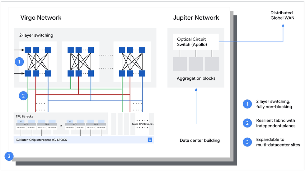
2. Figure 2: TPU 8t rack level connectivity to Virgo fabric This figure shows how TPU 8t scales to an astonishing 134,000 chips. The new Virgo Network is a flat, two-tier non-blocking topology that delivers up to 4x more data center network (DCN) bandwidth for large-scale training. In the diagram, racks are not only interconnected through high-radix switches but also connect to the Jupiter north-south optical network. This effectively addresses the long-tail latency caused by too many network tiers in million-parameter-scale cluster training.
3. Figure 3: TPUDirect Storage data path comparison This is the key comparison that eliminates the "I/O pain point". The top half shows the conventional architecture, where data must pass through the host CPU and DRAM, a severe bottleneck when ingesting huge multimodal datasets. The bottom half shows the new architecture with TPUDirect Storage: using RDMA, data flows directly from 10T Lustre high-speed storage into the TPU's HBM (6,528 GB/s of bandwidth), bypassing the CPU entirely. Test data show storage access is a full 10x faster than the previous-generation Ironwood TPU, keeping the compute cores constantly fed.

4. Figure 4: TPU 8i ASIC block diagram Moving to TPU 8i, built for inference and sampling, the design looks completely different from 8t. The biggest physical highlight is 384 MB of on-chip SRAM (Vmem), 3x the previous generation (and far more than 8t's 128 MB). In long-context agentic inference, larger SRAM can hold the entire KV cache on-chip, dramatically reducing core idle time. In addition, SparseCore is replaced by the new CAE (Collectives Acceleration Engine). The CAE handles the cross-core synchronization and reduction steps required by autoregressive decoding and chain-of-thought, cutting on-chip collective latency by 5x.

5. Figure 5: TPU 8i hierarchical Boardfly topology This is the most exciting interconnect change in the entire paper. TPU 8i abandons the traditional 3D torus in favor of a high-radix hierarchical topology called Boardfly. The diagram has three levels: 4 chips form a building block, and 8 boards are fully interconnected with copper cables into a group. Here's the key point: at the top-level pod, 36 groups (up to 1,024 chips) are interconnected through OCS (Optical Circuit Switches). Pushing optical communications and OCS down into the foundational interconnect backbone proves that for MoE workloads with frequent all-to-all cross-node communication, traditional electrical switching can no longer meet latency requirements, and optical switching has officially become the lifeline of future cluster scaling.

6. Figure 6: The Boardfly vs. torus math (max 7-hop latency visualized) This figure proves the decisive advantage of Boardfly with OCS in the most direct numbers. In a conventional 1,024-chip 3D torus (8x8x16), the farthest nodes are (8/2) + (8/2) + (16/2) = 16 hops apart. With Boardfly and OCS, the network diameter is compressed to at most 7 hops. That 56% reduction in hops translates directly into much lower tail latency, so the model no longer stalls waiting on network packets when dynamically dispatching to different experts.

Conclusion Google's eighth-generation TPU is not just another round in the compute arms race; it marks a major watershed in infrastructure philosophy. TPU 8t uses extreme scale-out networking and direct-attached storage to deliver the brute-force throughput future world models will need, while TPU 8i uses massive SRAM and a forward-looking OCS-based topology (Boardfly) to precisely break the all-to-all latency pain point of MoE architectures. For the industry, this deep dive makes one thing clear: the decisive battleground for future AI hardware has shifted from raw logic compute to deep optimization of "optical interconnect" and the "memory hierarchy".
(Disclaimer: All technical articles on this site are for technology and industry trend analysis only and do not constitute investment advice of any kind.)


Comments