


Technical Paper Analysis | When XPU Heat Sits Directly on the Photonic Chip: imec Quantifies the Thermal Cost of 2.5D/3D CPO in 18 Figures
When the optical engine moves onto the same interposer as the GPU, or is even stacked directly beneath it, you save the power and latency of electrical interconnect, but in exchange you get a harsh physical fact: temperature-sensitive ring/disk modulators now live directly under the XPU's heat chimney. What this imec paper does is quantify that "thermal cost" number by number, using CFD plus finite-element simulation.
This thermal modeling study by imec (Coenen et al.), published in IEEE TCPMT, fully benchmarks the thermal behavior of two Co-Packaged Optics (CPO) architectures: 2.5D (OIO2.5D, optical engine and XPU side by side on the same interposer) and 3D (OIO3D, XPU hybrid-bonded directly on top of the photonic chip).
On the cooling side, Si microchannel (µchannel) liquid cooling yields a convective heat transfer coefficient (HTC) of about 7×10⁴ W/m²-K; using this as the boundary condition, the system's "thermal wall" falls at 819–1441 W/XPU, and is extremely sensitive to the XPU power map (the CPU type is about 300 W lower than the GPU type, and uniform power is double the CPU type).
The real payoff is in the second half: moving from 2.5D to 3D, the amplitude of thermal crosstalk from the XPU to the photonic chip jumps from 8 K to 60 K, the spatial gradient rises from 0.9 K/mm to 12 K/mm (13x), and the temporal gradient rises from 0.03 K/ms to 1.78 K/ms (60x).
These three numbers directly determine the pre-heating power for ring modulator thermal tuning, how fast the controller must track, and whether temperature sensors can be shared. 3D integration is the winner electrically, but this paper marks it as the loser in thermal management.
1. Paper Background: Who Did It and Why It's Worth Reading
"Benchmarking the Thermal Impact of 2.5D/3D Co-Packaged Optics on Si Photonic Devices," by David Coenen, Herman Oprins, Yoojin Ban, and Joris Van Campenhout of imec, has been accepted by IEEE Transactions on Components, Packaging and Manufacturing Technology (TCPMT) (DOI: 10.1109/TCPMT.2026.3705221).
imec's Optical I/O industrial affiliation program is a global hub for silicon photonics thermal and packaging research. Over the past few years this team has built up a long series of papers on disk modulator thermal behavior, hybrid bonding thermal resistance, and dynamic compact models of ring modulators (Coenen alone appears on seven or eight papers in this paper's reference list). So this is not an isolated simulation exercise but the latest culmination of a mature thermal modeling framework.
The reason it's worth reading is simple: the industry keeps pushing to move optics "into the belly of the chip" (scale-up architectures, SiPh interposers, 3D stacking), but nearly all discussion focuses on bandwidth, energy efficiency, and pJ/bit. This is one of the few studies that pins down, in quantifiable numbers, exactly how much hotter 3D makes the photonic chip.
2. The Core Question in One Sentence
When XPU power density reaches about 1 W/mm² and must be held in check by wafer-level liquid cooling, how does that heat reach the temperature-sensitive silicon photonic modulators, and how much do 2.5D and 3D differ?
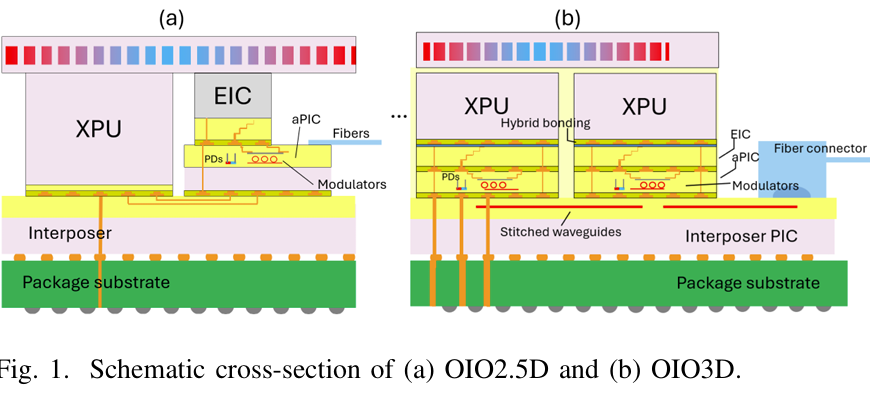
3. Anatomy of the Two Packages: Architecture and Benchmark Map (Figure 1–2)
This figure shows cross-sections of the two packages. OIO2.5D places the SiPho engine (a PIC chip with an EIC driver chip hybrid-bonded on top) side by side with the XPU on the same Si interposer; OIO3D hybrid-bonds the XPU directly onto an active PIC (aPIC) and EIC stack, then bonds the whole assembly onto a passive PIC (pPIC) interposer, using SiN waveguides in the pPIC to optically interconnect many XPU tiles. The key difference is obvious at a glance: in 2.5D the photonic chip sits "beside" the XPU; in 3D it sits "directly beneath" it.
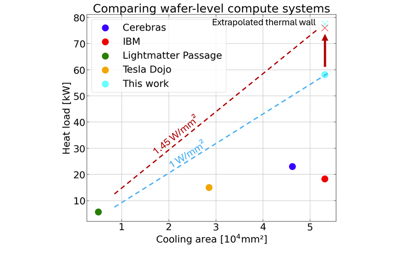
This figure surveys wafer-scale computing systems already in the industry, plotting their total power against available cooling area, and names four examples: IBM, Cerebras (WSE-3), Lightmatter (Passage), and Tesla (Dojo). The paper uses it to define the "thermal wall": these systems will eventually hit a wall where performance is capped by the maximum junction temperature for reliable operation. imec's setup is a pPIC interposer filled with 56 optically interconnected XPU tiles at 700 W each, giving an average power density of about 1 W/mm², consistent with the literature; pushing power up to the thermal wall reaches 1.45 W/mm². Its significance: it anchors the academic model in the power/area coordinates of real products rather than in thin-air assumptions.
4. Building the Model: Finite-Element Mesh and Multiscale Refinement (Figure 3–4)
This figure shows the finite-element (FE) model of the OIO2.5D package, with the XPU, PIC, and EIC stacked on the interposer substrate, plus (b)(c) showing the mesh progressively refined in the region of interest. The challenge is bridging device scale (µm-scale disk modulators) and package scale (cm-scale interposer) at the same time, which requires multilevel mesh refinement. The paper exploits package symmetry to shrink the simulation domain: OIO2.5D includes only one SiPho engine, with only one disk modulator in the PIC; a 0.1 K/W thermal resistance at the bottom of the interposer represents heat dissipation into the package substrate, so most heat is removed by the top cooler. The PIC chip is 5×5 mm² and the EIC chip 1.5×2 mm².
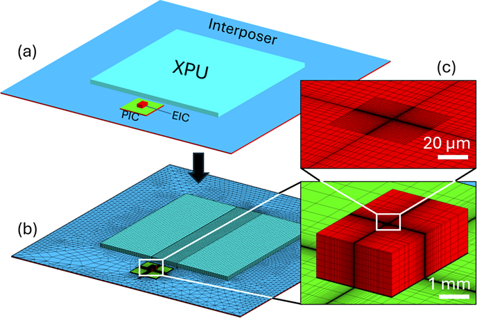
This figure shows the OIO3D FE model and mesh details of its 1/4 symmetric slice. The 3D case uses quarter symmetry across the wafer, with each tile at 25×25 mm². These two model figures are mostly engineering detail; the point they convey is this: imec uses symmetry plus multiscale meshing to compress a heat transfer problem spanning four orders of magnitude into a computable size, with thermal simulation in MSC Marc and flow in Ansys Fluent. This is the foundation for the credibility of every number that follows.

5. An Underrated Source of Thermal Resistance: The Hybrid Bonding Interface (Figure 5)
This figure shows how the hybrid bonding interface is modeled: (a) a unit cell of the interface, showing only the Cu with the dielectric hidden for clarity; (b) a 1/4 symmetric slice; (c) the temperature contour with heat flux q applied at the bottom; (d) the disk modulator model, marking three different bonding regions. Because the structure repeats at a 10 µm pitch, an equivalent thermal resistance R = t/λ = ∆T/q can be extracted from the unit cell and converted into an equivalent thermal conductivity, greatly simplifying the overall model.
Here lies an easily overlooked design variable. Table I gives the equivalent thermal resistance of the three bonding regions: 0.48 for the active region with vias, 0.94 for the dummy region without vias, and 1.85 mm²-K/W for the dielectric-only no-fill region: the same bonding layer can differ in thermal resistance by nearly 4x depending on whether it has copper and vias. Because the device pitch is only 100 µm and the bond pad pitch only 10 µm, the paper precisely models only the bond pads directly connected to the disk modulator and uses an equivalent thermal conductivity for the rest. This shows that in a 3D stack, the metal fill ratio of the bonding layer is itself a thermal design lever.

6. Where the Heat Comes From: CPU and GPU Power Maps (Figure 6)
This figure shows the two XPU power maps used in the simulations, both at about 700 W total: (a) a multi-core CPU mock-up with 36 cores and local power density as high as 3 W/mm²; (b) a GPU mock-up with a more uniform power distribution and a lower peak power density of about 1.8 W/mm². Beyond the XPU, aPIC and EIC power depend on link energy (pJ/bit) and total bit rate; the paper uses 0.426 W/mm² for the EIC and 0.113 W/mm² for the aPIC.
This plain-looking figure is actually the cause behind every conclusion in the second half of the paper. The CPU's "small cores, high density" versus the GPU's "large cores, low density" directly determines the thermal wall height and the spatial distribution of thermal crosstalk; as we will see, the photonic chip's temperature is almost an imprint of the XPU power map.

7. The Physics of Cooling: Si Microchannel Liquid Cooling (Figure 7–8)
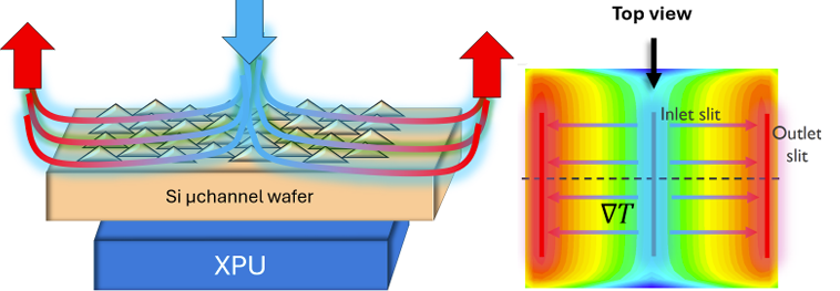
This figure shows the concept of the Si microchannel cooler: each XPU tile has a coolant inlet slit at its center, where the flow splits in two, runs in parallel toward both sides, and collects at outlet slits at the edges. This flow configuration creates a caloric thermal gradient across the XPU: the coolant heats up as it absorbs heat along the way, so the inlet end is cool and the outlet end is hot. The design is inspired by IBM's wafer-scale microchannel work.
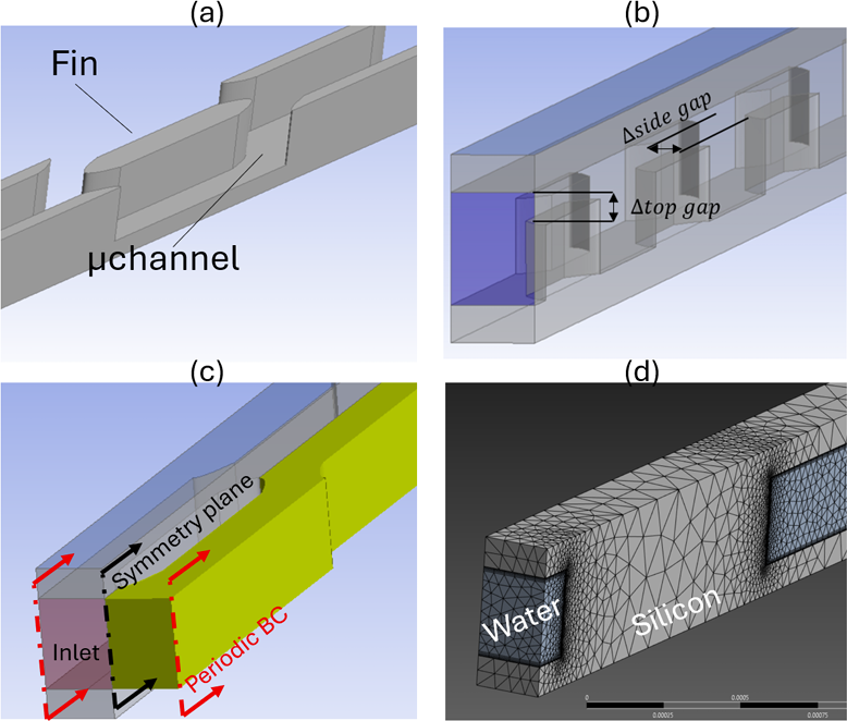
This figure shows the microchannel geometry and model simplifications: (a) the channels are the negative space between Si fins, which increase heat transfer area, promote fluid mixing (mostly in the laminar regime), and disrupt boundary layer buildup; (b) the two swept geometric parameters, fin side gap and top gap; (c) symmetry planes and periodic boundaries to further shrink the model; (d) the mesh, with 800,000 elements for a single 14 mm-long microchannel. The paper assumes a very low thermal contact resistance (0.2…2 mm²-K/W) between the XPU's Si substrate and the Si microchannel cooler, corresponding to wafer-to-wafer bonding with an oxide layer.
8. Quantifying Cooling Performance: How HTC Is Extracted and Where the Trade-Off Lies (Figure 9–11)
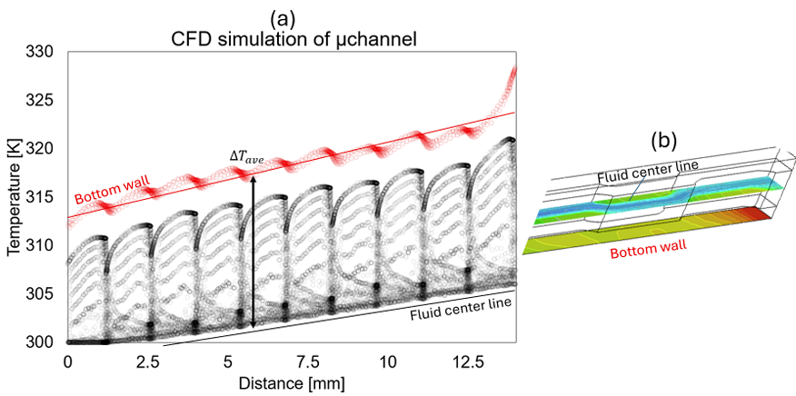
This figure shows how the HTC (convective heat transfer coefficient) is extracted. (a) plots the cooler bottom wall temperature (red) and the fluid temperature at the channel's central plane (black), taken at the mid horizontal plane; the spread in fluid temperature reflects the internal gradient from the center streamline to near-wall streamlines. The coefficient is calculated as HTC = q/∆T, using the ∆T between the bottom wall and fluid center temperatures averaged along the flow. (b) shows temperature contours on the bottom and central planes. This step is key to the whole cooling model: it condenses complex 3D conjugate heat transfer into a single HTC number usable as a boundary condition.
This figure shows the CFD static pressure and temperature fields: (a) static pressure, (b) temperature with a 240 µm side gap, (c) temperature with a 0 µm side gap. Comparing (b) and (c) shows intuitively how the gap changes heat and flow distribution.

This figure shows CFD results for multiple microchannel designs, each swept over inlet velocities of 1.5–3.5 m/s: (a) HTC vs pressure drop, (b) total temperature drop (convective + caloric) vs pumping power, (c) normalized cooler thermal resistance. At its core is a clear trade-off curve: channels without top/side gaps have the highest HTC, but at the cost of extremely high flow resistance. The paper takes a conservative HTC = 7×10⁴ W/m²-K as the reference for subsequent simulations. From (b): at an input power density of 1 W/mm², ∆T ≈ 20 K in the cooler is a good target, with convective and caloric thermal resistance each accounting for about half.

9. The Full Package Temperature Field and the Thermal Wall (Figure 12–14)
This figure shows package cross-section temperature contours (relative to coolant inlet temperature) for OIO2.5D (a) and OIO3D (b), with an inset of a disk modulator with local substrate undercut (UCUT). Stacking the EIC on the PIC affects the thermal behavior of SiPho devices, most notably reducing heater efficiency as heat spreads vertically into the EIC. This figure is the first to visualize the difference: the photonic chip in 2.5D stays relatively cool, while in 3D it is immersed directly in the XPU's thermal field.

This figure shows OIO3D temperature contours (top view): (a) the cooler, (b) the full wafer with 56 XPUs, (c) CPU, (d) GPU. The key observation: the temperature fields of all XPUs across the wafer are almost identical. That's because top-side liquid cooling is so effective that nearly all heat leaves through the top with very little lateral spreading, so each XPU is effectively independent, with no significant lateral thermal coupling between them. This matters for the later conclusion that thermal crosstalk is independent of the number of XPUs.

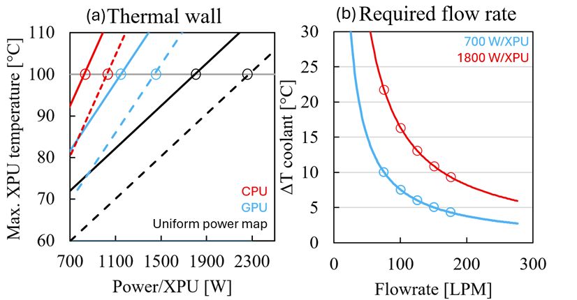
This figure quantifies the "thermal wall": (a) maximum system temperature vs XPU power, extrapolated to find the power at which maximum junction temperature reaches 100°C, defined as the thermal wall (solid lines OIO3D, dashed lines OIO2.5D, three power maps); (b) OIO3D coolant temperature rise vs total flow rate. Table II gives the full numbers:
Power map: Uniform; OIO2.5D thermal wall: 2285 W; OIO3D thermal wall: 1812 W
Power map: GPU; OIO2.5D thermal wall: 1441 W; OIO3D thermal wall: 1152 W
Power map: CPU; OIO2.5D thermal wall: 1028 W; OIO3D thermal wall: 819 W
Three hard conclusions: First, the thermal wall is extremely sensitive to the power map: the thermal wall for uniform power is double that of the CPU type. Second, the GPU type is about 300 W higher than the CPU type, because GPU cores are large and average power density is lower. Third, OIO2.5D's thermal wall is about 200–300 W higher than OIO3D's, because in 3D the EIC + aPIC share of I/O power is stacked beneath the XPU and counted together with it; moving I/O power off-chip actually raises the XPU's thermal wall, a substantive advantage of 2.5D. For coolant flow, a rule of thumb emerges of "about 1 LPM per 1 kW of XPU power" (700 W/XPU needs 74 LPM to keep caloric ∆T below 10 K; 1152 W needs 110 LPM).
10. The Main Event: Spatial Characteristics of XPU-to-PIC Thermal Crosstalk (Figure 15–17)
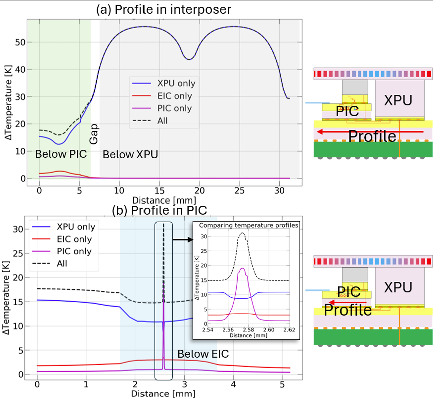
This figure shows OIO2.5D temperature profiles: (a) the interposer substrate, (b) inside the PIC. There are two conclusions. First, when only the PIC or only the EIC is powered, the temperature profile drops to zero beneath the XPU, proving that thermal coupling from the optical engine back to the XPU is negligible and supporting the model's use of a single optical engine. Second, zooming into the PIC reveals a local temperature peak at the disk modulator with its active heater. Average thermal crosstalk from the XPU to the PIC is 11 K, but at the SiPho devices it drops to 8 K thanks to the local UCUT: the UCUT is meant to block heat flow into the Si substrate to improve heater efficiency, and here it also partially blocks heat coming from the substrate in the opposite direction.
This figure shows OIO3D temperature profiles for the CPU (a) and GPU (b) power maps, spanning both the XPU and PIC layers. Key finding: PIC temperature closely tracks the XPU temperature profile, because vertical thermal coupling between the two layers in a 3D stack is extremely strong. This means any variation in the XPU power map gets imprinted onto the PIC as a strong thermal gradient. The CPU, with its high core power density, has higher peak core temperatures than the GPU; in the GPU case, PIC temperature is even higher than GPU temperature throughout, because the PIC sits beneath the XPU and nearly all heat leaves through the top.

This figure shows PIC-layer temperature contours for OIO2.5D (a) and OIO3D (b), used to calculate the maximum spatial temperature gradient caused by XPU crosstalk. The results are summarized in Table III:
Metric: crosstalk amplitude ∆T; OIO2.5D: 8 K; OIO3D: 60 K
Metric: spatial gradient ∇T_space; OIO2.5D: 0.9 K/mm; OIO3D: 12 K/mm
Metric: temporal gradient ∇T_time; OIO2.5D: 0.03 K/ms; OIO3D: 1.78 K/ms
The spatial gradient is 13x higher in 3D than in 2.5D, and crosstalk amplitude worsens from 8 K to 60 K: that is the penalty for 3D integration of the PIC with the XPU. And because lateral thermal coupling between XPUs is negligible, these gradients do not depend on how many XPUs in OIO3D are powered at the same time.

11. The Time Dimension: Start-Up Transients and a 60x Temporal Gradient (Figure 18)
This figure shows transient simulation of system start-up (thermal step response): (a) normalized PIC temperature response when each layer is powered separately, (b) absolute PIC ∆T during full start-up (OIO2.5D vs OIO3D). Three time constants span an extremely wide range: the device level is fastest at 21 µs; next comes EIC crosstalk at 13 ms; and finally XPU crosstalk at 29 ms for OIO3D and 295 ms for OIO2.5D. PIC and EIC responses are almost unaffected by the package architecture, but XPU crosstalk is about 10x slower in 2.5D.
Smaller amplitude times slower response makes OIO2.5D's temporal temperature gradient a full 60x smaller. This is a major drawback of 3D: a steep 1.78 K/ms gradient must be compensated in real time by ring thermal tuning, and a 60x larger gradient pushes controller design difficulty to the maximum. The paper also suggests a way out: replacing ring/disk modulators with GeSi electroabsorption modulators, which are far more tolerant of temperature changes.

12. Technical Highlight: Translating "Thermal Cost" Into Circuit Design Language
The paper's most elegant step is converting abstract temperature numbers directly into specs that photonics and circuit designers understand:
Absolute thermal crosstalk → pre-heating power. To keep a ring modulator wavelength-locked across the full 0–100% range of XPU power, the gap between 8 K and 60 K of pre-heating is roughly 0.6 mW vs 5 mW for a disk modulator, or 0.02 pJ/bit vs 0.17 pJ/bit for a 28 Gbps link. 3D thermal crosstalk directly eats a large chunk of the energy-efficiency budget.
Temporal gradient → minimum controller tracking speed. 0.03 K/ms (2.5D) vs 1.78 K/ms (3D) sets the minimum response time of the temperature controller; a 60x gap is a hard constraint on the control loop.
Spatial gradient → whether temperature sensors can be shared. Assuming a temperature variation of 0.15 K is allowed to maintain wavelength lock, OIO3D devices can share a temperature sensor only within 12.5 µm of each other, while OIO2.5D relaxes this to 167 µm. This effectively means 3D almost requires individual thermal tuning for every device, sharply raising sensing and control costs.
13. Industry Implications: What This Means for the CPO Volume-Production Roadmap
First, to be clear about positioning: this is a simulation study, not production data, but it delivers trend direction rather than absolute values, and the methodology is solid enough that the direction is credible.
In the industry context, several points are worth noting:
First, 3D is not a free lunch. The industry talks about SiPh interposers, scale-up, and moving optics into the belly of the chip as if they were the inevitable endgame, but this paper labels the thermal cost clearly: 3D wins on electrical latency and power, yet worsens across the board in thermal crosstalk (8→60 K), spatial gradient (13x), and temporal gradient (60x). Anyone pursuing 3D has to work out the costs of thermal tuning, controllers, and sensor density first. We give a fuller industry perspective on this "electrical vs packaging" trade-off in [Technical Paper Analysis | CPO Is Won in Packaging, Not Optics: John Lau Explains Every Approach to PIC/EIC Heterogeneous Integration] (in Chinese).
Second, 2.5D's value gets repriced. Moving I/O power off-chip raises the thermal wall, with 7x less thermal crosstalk and a 60x smaller temporal gradient: in thermal management, 2.5D is actually the more pragmatic transitional option. This also ties into the debate over when scale-up will truly arrive; for related context see [The 3D Photonic Integration Watershed: OpenLight's CEO Breaks Down Five Convergence Thresholds, and Why Scale-Up Is CPO's Real Window] (in Chinese).
Third, cooling and packaging are the same problem. An HTC of 7×10⁴ W/m²-K, about 1 LPM per kW, and a 4x thermal resistance gap from hybrid bonding metal fill all point to one thing: CPO thermal design cannot wait until packaging is finalized; it must be co-designed together with bonding, microchannels, and the interposer. This is a microcosm of how, amid the wave of optical communications becoming "semiconductorized," packaging and thermals are moving from behind the scenes to the core of the value chain.
Fourth, modulator choice will be driven by thermals. The paper explicitly recommends GeSi electroabsorption modulators as a high-temperature-tolerant alternative. If the 3D thermal environment really pushes ring/disk modulator control costs out of hand, the modulator technology roadmap may shift as a result, a signal worth tracking over the long term.
14. Conclusion
The value of this paper lies not in calculating some elegant new architecture, but in honestly laying the thermal costs of 3D CPO on the table one by one: crosstalk from 8 K to 60 K, a 13x spatial gradient, and a 60x temporal gradient. While the entire industry narrative races toward "stacking optics into the chip," this imec paper is like a tap on the brakes: not saying 3D can't be done, but that a 3D photonic chip now lives directly beneath the XPU's heat chimney, and every cost of wavelength locking, controllers, and sensor density has to be repriced.
The one-line takeaway: in the world of CPO, heat is no longer the thermal engineer's problem alone; it is now a spec that photonics and circuit designers must sign off on together. Whoever first treats heat as a first-class citizen in co-design will be first to reach the real volume-production window for 3D optical interconnect.
References
David Coenen, Herman Oprins, Yoojin Ban, Joris Van Campenhout, "Benchmarking the Thermal Impact of 2.5D/3D Co-Packaged Optics on Si Photonic Devices," IEEE Transactions on Components, Packaging and Manufacturing Technology (TCPMT), 2026. DOI: 10.1109/TCPMT.2026.3705221. (imec, Kapeldreef 75, Leuven, Belgium)
D. Coenen et al., "Thermal Challenges for Disk Modulators in Optically-Connected System-on-Wafer," IEEE JSTQE, Vol. 32, No. 2, Dec. 2025.
D. Coenen et al., "Thermal modeling of hybrid three-dimensional integrated, ring-based silicon photonic–electronic transceivers," J. of Optical Microsystems, Vol. 4, No. 1, 011004, Jan. 2024.
E. G. Colgan et al., "Fabrication and Performance of 300-mm Wafer-Scale Silicon Microchannel Cooler," IEEE CPMT, Vol. 13, No. 4, April 2023. (Source of the microchannel cooling design)
H. Oprins et al., "3D Wafer-to-Wafer Bonding Thermal Resistance Comparison," ITherm, Orlando, July 2020. (Hybrid bonding thermal resistance method)
Related Reading
[Technical Paper Analysis | CPO Is Won in Packaging, Not Optics: John Lau Explains Every Approach to PIC/EIC Heterogeneous Integration] (in Chinese) (internal Wix link, to be added at upload): places this article's thermal costs in the full packaging picture of PIC/EIC heterogeneous integration
[The 3D Photonic Integration Watershed: OpenLight's CEO Breaks Down Five Convergence Thresholds, and Why Scale-Up Is CPO's Real Window] (in Chinese) (internal Wix link, to be added at upload): an industry view on when 3D/scale-up will arrive
[ECTC 2026 | imec | Wafer-to-Wafer Hybrid Bonding Technology with 200nm Interconnect Pitch] (in Chinese) (internal Wix link, to be added at upload): the same imec team's latest progress on hybrid bonding technology
(Note: this article contains 18 in-place [image] annotations and several tables. Before publishing, add the corresponding paper Figure images in the Wix dashboard; tables have been flattened into text and can be converted back into tables in the dashboard if needed.)


Comments