


Paper Analysis | Building a 1.6T Optical Engine with Fan-Out Packaging: Singapore A*STAR's Low-Cost CPO Approach
CPO (Co-Packaged Optics) has been debated for nearly a decade, and what has really held back volume production was never “can optics sit next to electronics,” but “once they're together, is the package expensive, is it easy to make, and can it be tested on a full wafer and shipped like an electronic chip?”
This paper, published in the February 2025 issue of the Journal of Lightwave Technology and selected as a Top-Scored Paper, gives a direct answer: don't take the expensive road. No TSV, no glass — instead it uses a mature process the electronics packaging world has run for over a decade, FOWLP (Fan-Out Wafer Level Packaging), to build an 8-channel, 200G-per-channel, 1.6T silicon photonic engine, with both NRZ and PAM4 working.
CPO's real bottleneck isn't “how to combine optics and electronics,” but “whether the combination can be mass-produced cheaply.”
1. Background: Three Singapore Teams, One Sovereign Silicon Photonics Supply Chain
The authors span three organizations, each a key node in Singapore's A*STAR (Agency for Science, Technology and Research) ecosystem:
Rain Tree Photonics: the fabless design company responsible for the silicon photonic engine and system validation; corresponding author Xin Li is here.
IME A*STAR (Institute of Microelectronics): responsible for developing the FOWLP advanced packaging process.
Advanced Micro Foundry (AMF): Singapore's silicon photonics foundry and the actual fab for the PIC (Photonic IC).
Viewed together, the point isn't just one paper — it's that Singapore is using an integrated “design + packaging + foundry” chain to build a silicon photonics supply chain independent of the big US players. The research was funded by A*STAR's Science and Engineering Research Council (Grant I2001E0071) — a national-team playbook.

2. The Core Question: Three Paths for CPO Packaging, and Why Pick the Least Sexy One
The paper opens by comparing three advanced packaging routes side by side. This section is the soul of the paper and the judgment STT readers should take away:
TSV-based (through-silicon via): the highest integration density and shortest signal path, but TSV processing is complex and very expensive at low volume, making it a poor fit for “high-mix, low-volume” silicon photonic transceivers.
Glass-based (glass substrate): strong performance, but high manufacturing cost, and a glass interposer can't embed EIC/PIC bare dies, which limits integration density.
FOWLP (Fan-Out Wafer Level Packaging): mature, low-cost and high-yield, and like TSV it can embed bare dies in the interposer; it has mainly been used for electronic chips such as smartphone processors, and using it for optical engines means solving the problem of keeping the optical coupling uncontaminated.
In other words, TSV is too expensive and glass can't embed dies, while FOWLP is the route that is “already proven in volume electronics packaging with the lowest unit cost.” What the paper sets out to prove is that this cheap route can also carry 200G/lane high-speed optical signals.
3. Key Figures, One by One
This figure shows the clever “wire-bond-free” structure of the FOWLP optical engine

The core of the design is eliminating wire bonds. The traditional approach connects the EIC and PIC with gold wires, which are parasitic inductance and signal killers. Here the EIC is flip-chipped directly onto the PIC's RF I/O pads, making the path as short as it can be — for high-speed parts like drivers and TIAs (Transimpedance Amplifiers), that is the foundation of signal integrity.
The embedded TMV (Through Mold Via) is the backbone of the structure: a 150 µm laser-drilled hole tapering to about 60 µm at the bottom and landing on the front-side RDL copper, connecting the top and bottom of the package while supporting 200G/lane high-speed signals.
This figure shows how the process avoids “damaging the optical eye”

The hardest hurdle in using FOWLP for optical engines: once the packaging epoxy molding compound (EMC) touches the PIC's optical coupling facet (SSC, Spot Size Converter), coupling efficiency is ruined. The paper's solution is low-tech but effective — a “silicon buffer breakwater” structure that acts like a dam to stop EMC from flowing onto the SSC. Dicing then exposes the SSC for edge coupling.
Result: coupling loss < 2 dB/facet, without index-matching epoxy, almost identical to bare-die test results (Fig. 7). This effectively proves FOWLP packaging doesn't eat into optical performance.
This figure shows it “can be auto-tested like a silicon wafer”
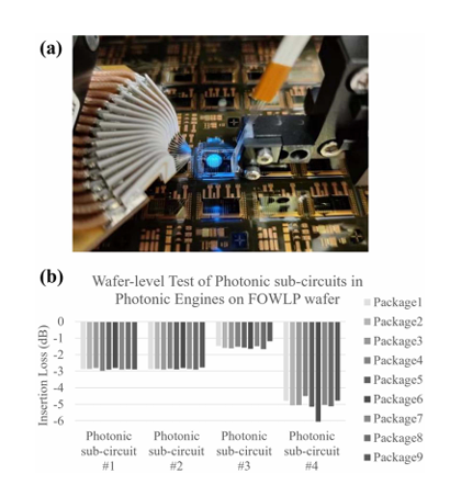
For volume production, this matters more than the technical figures. The FOWLP process preserves the PIC's vertical grating couplers, so the whole packaged wafer can go on an automated prober for high-speed testing just like an ordinary silicon wafer — 35 of 36 passed. For “high-mix” applications like CPO, whether you can auto-test at wafer level directly decides whether cost and yield can scale.
This figure shows RF loss low enough for “direct drive”

The 1.1 dB RF loss (including substrate routing) is what makes “direct drive” possible later — with low enough loss, the ASIC can drive the modulator directly through the substrate and package, eliminating the retimer/DSP in between.
4. Technical Highlight: LPO-Friendly — The Real Selling Point
The paper demonstrates two drive scenarios:
FRDL probing (emulating a co-packaged driver): 112 Gbaud NRZ eyes fully open with zero receiver equalization; 112G per channel, 896G aggregate.
Direct-drive (emulating an ASIC driving through the substrate): PAM4 needs only a 9-tap FFE to meet IEEE 802.3dj 200G/lane; NRZ shows excellent TDEC even without receiver equalization.

This is exactly what LPO (Linear Pluggable Optics) wants most — remove the DSP and retimer and rely on excellent signal integrity for direct linear transmission, saving power and cutting latency. The paper also highlights an advantage wire bonds can't match: the impedance of every interconnect segment inside FOWLP is “tunable by design”, so the next version can optimize impedance matching to further cut the number of FFE taps for direct drive. With wire bonds you only know the impedance “after bonding”; with FOWLP it's “decided when you draw it.”
5. Industry Link: How Far from Volume Production, and Who Benefits
Process maturity: FOWLP itself has been in volume production for smartphone chips for over a decade; 300 mm lines, KGD selection and C4 packaging all exist already. The technical risk lies mainly in “optical coupling protection” and “mixed optical-electrical testing,” and this paper has cleared both.
Scalability: the paper explicitly says it can scale up by “increasing PIC channel count” or “packing more PIC chiplets into the FOWLP”; 1.6T is not the ceiling.
Beneficiaries: for players needing low-cost, high-mix silicon photonics packaging — especially second-tier vendors and newcomers who want to avoid the high-end 2.5D route of TSMC COUPE / Broadcom — FOWLP offers a shortcut that “works on mature electronics packaging lines.” For Taiwan's OSATs and silicon photonics startups, this is a route worth benchmarking.
6. Verdict: In CPO's Cost War, FOWLP Casts a Key Vote
The paper's historical position is clear: it isn't competing on whose optical engine is faster, but proving that “a cheap packaging route can also carry 200G/lane.” Where TSV is too expensive and glass can't embed dies, FOWLP uses a silicon breakwater plus through-mold vias to turn an extremely mature fan-out packaging line into a volume-production candidate for CPO/LPO.
For the whole supply chain, the real signal is: CPO competition is shifting from “can it be built” to “who can build it cheaply.” And Singapore, with a sovereign design–packaging–foundry chain, has already cast that vote.



Comments