


OCP Global Summit 2026 | Quintessent | Alan Liu | Quantum-Dot Laser Sources for Slow-and-Wide
1. Why slow-and-wide pushes the pressure onto the laser
Slow-and-wide replaces a few high-speed lanes with many slower ones, cutting energy per bit and the SerDes burden. Liu opened with just two points: every optical link is powered by a laser, global laser capacity is tight, and almost all of it is InP.
The second layer of pressure comes from architecture. Scale-up architectures such as OCI use multi-wavelength DWDM, with several wavelengths on one fiber. We broke down that spec in Meta, Broadcom and AMD define the OCI 200G line-side spec: as the wavelength count grows, the "one DFB per wavelength" approach multiplies laser count, wavelength-control loops and package coupling points.
Quintessent's answer rests on three pillars:
Material: InAs quantum dots on GaAs substrates instead of InP quantum wells
Heterogeneous integration: the quantum-dot gain layer is bonded onto silicon photonics wafers, and silicon defines the laser cavity
Architecture: the same process makes single-wavelength DFBs or multi-wavelength comb lasers by changing only the silicon mask
2. Breaking down the material: borrowing the VCSEL GaAs ecosystem
Liu deliberately placed quantum dots in a familiar context: this GaAs material ecosystem is the same one that has powered Face ID VCSELs for almost a decade. Quintessent is fabless, outsourcing epi and processing; the epi partner he named on stage is IQE.
The numbers on the slides:
Epi on up to 6-inch GaAs substrates, with six 6-inch wafers per growth run (stated verbally)
More than 750 wafers grown to date
EVT phase, 100% foundry flow: Epi1 946 lasers, Epi2 1,019, Epi3 988, about 3,000 in total
Unoptimized WPE clusters at 25–30% in every lot
Reliability is preliminary data: a lot of Fabry-Perot quantum-dot lasers started aging in 2023 at 80°C and 125 mA (the realistic operating current for 30 mW output). It has passed 22,000 hours, about 2.5 years, with the bias current needed for 30 mW drifting within roughly ±5%. A new campaign with more than 150 devices and higher acceleration factors has started, and will scale to thousands before a full mean-time-to-failure model can be built.
22,000 hours shows the material does not degrade easily; it is not yet a product failure rate.
3. Breaking down the process: the four steps removed are InP's four challenges

▲ Quintessent's five-step heterogeneous integration flow: pattern SOI, grow quantum-dot epi, bond face-down, remove the GaAs substrate, test at wafer level (Image source: Quintessent | 2026 OCP Global Summit presentation)
A silicon photonics foundry first patterns waveguides, gratings and couplers in SOI, while quantum-dot epi is grown on 6-inch GaAs. The two wafers are bonded face to face with no alignment needed, the GaAs substrate is removed, and the thin quantum-dot film left on silicon goes through III-V processing.
The three lines at the bottom of that slide carry the most industrial meaning in the talk:
No facets: every laser gets optical and electrical tests on the wafer and ships as a known-good die
No e-beam, no regrowth: the cavity is defined by silicon photonics lithography at 65 nm or better
No InP: the gain material is entirely GaAs-based
Conventional InP DFB gratings need e-beam or holographic exposure, buried regrowth and cleaved facets before testing. Quintessent swaps these narrow steps for existing capacity at silicon photonics foundries and GaAs epi houses, which answers its "laser shortage" claim more directly than any single optical metric.
4. Breaking down the comb laser: no wavelength control needed, not enough power yet

▲ A single 3 × 0.25 mm silicon chip driven by a single current source produces 8 evenly spaced lines, with all channels drifting together with temperature (Image source: Quintessent | 2026 OCP Global Summit presentation)
The comb laser pitch is simple: one cavity, one bias, eight equally spaced lines, with no per-line tuning or feedback control. The slide data:
Chip size 3 × 0.25 mm; at 50 mA bias the eight lines sit within 2.0 dB
Uniform comb spectra from 20°C to 110°C
Peak WPE above 20%, more than 80 mW total in the silicon waveguide from the comb alone, no mode hops across bias
With an SOA, 200 mW total and more than 25 mW per wavelength (30°C)
Source | Total power | Per wavelength | Source note |
Comb laser (first shown at prior OFC) | ~40 mW | ~5 mW | Spoken "about half", STT calc |
Comb laser (this talk) | > 80 mW | ~10 mW | Slide p.10 |
Comb laser + SOA | 200 mW | > 25 mW | Slide p.11 |
8 × DFB + SOA array (200 GHz) | — | Up to 85 mW (single side) | Slide p.12 |

▲ Comb laser total power doubled in about seven months, but even with an SOA each wavelength is still about 25 mW, and that is on-chip power, not at the fiber (Image source: Simple Tech Trend original; data from Quintessent 2026 OCP Global Summit presentation)
The doubling deserves credit: in about seven months from the prior OFC to OCP, the comb alone went from roughly 40 mW (spoken estimate) to 80 mW. But the comparison needs one ruler. In CPO lasers do not have to chase 400 mW: NPO integrated lasers we discussed 400 mW-class single-wavelength CW lasers; that laser is split across many lanes. STT calc: split 8 ways gives about 50 mW per lane, 16 ways about 25 mW (excluding split loss). Each comb wavelength is already one lane, so 25 mW/λ only nominally matches a 16-way split, and it is still a chip-side number. The real comparison is how many milliwatts per lane survive into the fiber and through the ELSFP.
5. Isolators and DFB arrays: the half that can land before the comb
The single-wavelength DFB data from the same platform is actually more mature:
An 8 × DFB + SOA array at 200 GHz spacing, SMSR above 55 dB, mode-hop free, up to 85 mW single side, not yet optimized for power or efficiency
Five DFBs at different wavelengths (SOA biased at transparency, no gain) keep RIN near −150 dBc/Hz with optical feedback up to −15 dB
The point of the last item is that quantum-dot DFBs can likely run without an optical isolator when coupled to a PIC. Isolators are costly, bulky passive parts; removing them cuts BOM and simplifies assembly. Liu attributes this to the quantum-dot material's high tolerance to back reflection, but the slide's own word is "likely", so it needs link data with a real PIC before it is settled.
6. Risks and counterarguments
Absolute wavelength is not addressed yet. Lines that "drift together" only guarantee relative spacing. In Q&A Liu gave a temperature coefficient of about 0.08 nm/°C, consistent with the p.8 chart (lines move about 2 nm from 35°C to 60°C). STT calc: the OCI preview spectrum sits around 1,296–1,303 nm; 400 GHz is about 2.24 nm at 1,296 nm (2.29 nm at 1,311 nm). A 25°C rise moves the comb about 2.0 nm (about 0.9 slot), and about 28°C shifts it one full slot; across 20–110°C it moves about 7.2 nm, more than three slots. Either the microring modulators must track it or the source needs temperature control, which cuts into the claimed system simplification.
The spacing must be redesigned. Line spacing of this 8λ comb reads about 1 nm on the p.8 chart (about 180–185 GHz near 1,295 nm, STT calc). The OCI MSA version needs 4 wavelengths × 400 GHz with one comb per group; p.14 shows only a preview spectrum, with no power or uniformity data.
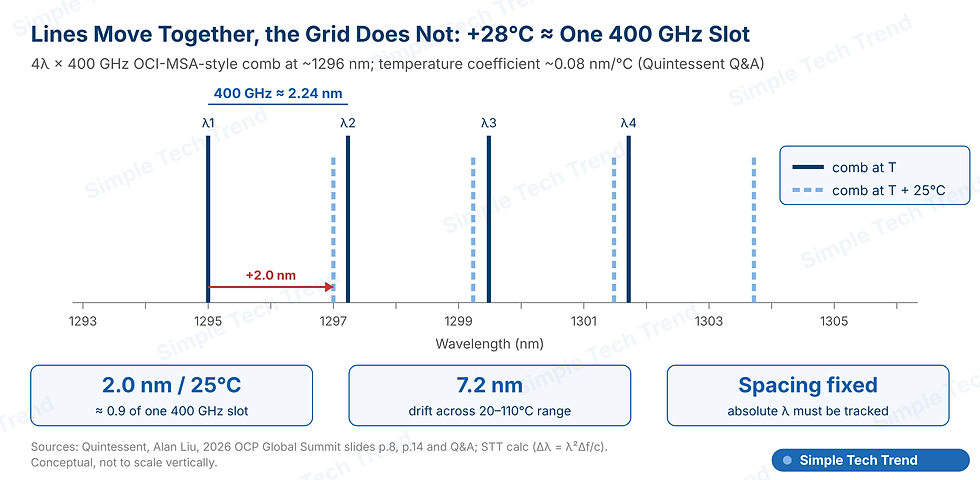
▲ At 0.08 nm/°C, a 25°C temperature rise shifts the whole 4 × 400 GHz comb by about 2.0 nm, roughly 0.9 of a channel spacing (Image source: Simple Tech Trend original; data from Quintessent 2026 OCP Global Summit presentation)
The reliability sample is still small. The 22,000 hours are preliminary data from one lot of Fabry-Perot lasers, not comb or DFB + SOA data; results from the 150-plus device campaign are not yet public.
The SOA adds new variables. The 200 mW relies on the SOA, and the slide itself notes that out-of-band SMSR still needs lower coupling loss and SOA optimization.
7. What it means for Taiwan's supply chain
This route pulls the laser from InP back to GaAs. Neither the slides nor the talk named any Taiwanese company; the only named epi partner is IQE. The relevance is the type of capacity rather than any one company: 6-inch GaAs epi and VCSEL-grade III-V processing are existing strengths of Taiwan's compound semiconductor foundries. If this route works, demand for laser gain material could spill from InP to GaAs lines, but no public information points to any specific Taiwanese company being involved.
Silicon photonics foundry and wafer-level bonding are another entry point. Quintessent's cavity is defined by silicon photonics lithography, so part of the laser's value moves to the SiPh foundry and bonding steps. This is the same OCI ecosystem described in ECOC2026 | Fast-and-narrow vs slow-and-wide: scale-up optics is decided by the SerDes at the chip edge.
For InP laser makers this is a mid-to-long-term substitution risk, not a near-term threat. At 25 mW/λ today, the first trials in 2027 are more likely in lower-power DFB arrays or pluggable DWDM transceivers.
8. Summary
The most convincing part of Quintessent's talk is not the eight-line spectrum but the manufacturing numbers: 3,000 lasers, 25–30% WPE, 22,000 hours. They show GaAs quantum dots bonded on silicon can run a foundry flow with wafer-level test, directly addressing tight laser capacity and the InP process bottleneck.
But slow-and-wide needs power per wavelength and absolute wavelength accuracy. The comb now delivers 25 mW per wavelength, measured on chip, which only nominally matches a 400 mW-class CW laser split 16 ways; at 0.08 nm/°C the whole comb shifts one 400 GHz slot for roughly every 28°C. Over the next 6–12 months, watch three things: measured power of the OCI-MSA-compatible 4 × 400 GHz source around OFC 2027, fiber-side power per wavelength in the ELSFP version, and the first results from the 150-plus device reliability campaign.
Wavelengths come eight at a time; milliwatts come one at a time. Quintessent's outcome depends on the latter.
This article is for technology and industry trend analysis only and does not constitute investment advice.


Comments