


Technical Paper Analysis | Polymer Waveguides Handle +20 dBm for Six Hours: The Missing "Optical Redistribution" Piece for ELS-Based CPO
The optical communications world is arguing about one thing: should CPO lasers go inside the chip? Integrating the laser into the silicon photonics chip gives the highest density and is the most attractive option; but the laser is the most failure-prone part of the whole system, and burying it in the package next to a GPU puts the most fragile component in the hardest-to-service spot. So another camp advocates an External Laser Source (ELS) — keep the laser outside the chip, and if it fails, just unplug it and swap it.
But external lasers carry a cost few like to talk about: you have to find a way to carry a +20 dBm-class high-power beam from the package edge to the modulators in the middle of the chip. And that light can't travel in silicon waveguides — at high power, silicon runs into two-photon absorption and free-carrier absorption, and beyond +20 dBm there's a risk of burnout. So what the ELS route really lacks is a channel that "can handle high power, is cheap, and can do optical redistribution."
This paper from AIST (Japan's National Institute of Advanced Industrial Science and Technology), published in the Journal of Lightwave Technology (May 2025), is a health check on exactly that channel. Conclusion first: single-mode polymer waveguides built on low-cost glass-epoxy (FR4) substrates carried +20 dBm CW light for six hours without degradation, with a temperature rise of only 4.4°C, and polarization extinction ratio at all four CWDM4 wavelengths passed the OIF specification. For the packaging camp, a long-missing piece of the puzzle has been filled.
1. What Problem This Paper Solves
In one sentence: can polymer waveguides withstand high-power ELS light fed directly into them?
AIST previously proposed a concept called the Active Optical Package (AOP) substrate — embedding silicon photonics bare dies in a conventional glass-epoxy substrate, then using polymer micro-mirrors and polymer waveguides for 3D optical redistribution, converting from fiber pitch (250 µm) to chip pitch (on the order of 30 µm). The problem was that they had only run preliminary tests at +24.6 dBm, without a full per-wavelength stability and reliability evaluation, and had never measured the polarization extinction ratio (PER) that matters most for ELS systems. This paper fills in those gaps one by one.

2. Key Figures, One by One
This figure shows that "the eight waveguides are nearly identical"

The eight waveguides made by Direct Laser Writing (DLW) held core dimension standard deviation to 0.14 µm (width) and 0.12 µm (height). For volume production, consistency matters more than a single impressive number — it means the process is reproducible, not a lucky pick. The material is Nissan Chemical's SUNCONNECT, and the substrate is commercially available high-Tg FR4.
This figure shows that "polarization-dependent loss is low enough"

PDL is a hidden killer in ELS systems — if the two polarization states see different losses when light couples from fiber into the chip, signal quality degrades. All eight waveguides showed PDL <0.5 dB across the band. Notably, the worst case this time (about 0.5 dB, Waveguide #7) was worse than the 0.25 dB of their previous single-sample paper, and the authors candidly explained why: this time the core is asymmetric (9 µm wide × 7 µm tall) rather than the previous symmetric square (8×8 µm), and measuring eight waveguides exposes process variation. This "no hiding the weak spots" attitude actually makes the data more credible.
This figure shows that "polarization extinction ratio passes the OIF threshold across the board"
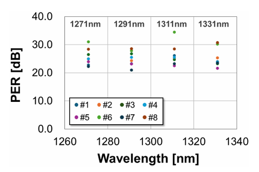
This is the pass line for ELS-based CPO. OIF requires PER >10 dB for 3.2T CPO modules; the average PER across the four wavelengths in this paper is 25–26 dB, with the worst at 21 dB — passing with more than 2x margin. As an alignment reference, butt-coupling the alignment modules directly (without a waveguide) measured 37 dB, the physical ceiling. In other words, the waveguide itself consumes only about 11–15 dB of polarization purity, still well above spec.
This figure shows "six hours at high power with no degradation" — the paper's signature result

This is the core value of the paper. They deliberately chose the "worst case" — assigning each wavelength to the waveguide with the highest loss at that wavelength — then fed +20 dBm CW light from an ELS supplied by Furukawa Electric for six hours. Result: input and output were highly linear with no excess loss, and output fluctuated only within ±0.3 dB (mainly from manual alignment error and PDL, not waveguide degradation). The power density inside the waveguide works out to about 180 kW/cm² — below the 250 kW/cm² safety limit for fiber, but firmly in high-power territory.
This figure shows that "heat isn't a problem at high power"


Many people's first reaction to "polymer" is "won't it get burned by the light?" AIST counted the entire 0.55 dB waveguide loss as heat (the most conservative assumption) and simulated a 4.9°C rise; the measured rise was 4.4°C, and the two agree. The substrate thermal reference is Resonac's MCL-E-705G. For packaging, 4.4°C is practically noise — this directly dismantles the most common objection that "polymers can't handle high power."
3. The Two Most Innovative Technical Points
First, moving "high-power tolerance" from silicon to polymer. Silicon waveguides above +20 dBm hit two-photon absorption and free-carrier absorption — a physical limit with no way around it. AIST's solution isn't to optimize silicon but to change materials: use polymer waveguides to carry the high-power light, and leave silicon photonics to do what it does best, modulation, so each material does what it's good at.
Second, using low-cost FR4 glass-epoxy substrates instead of expensive glass or silicon interposers. This is key to the cost story. The combination of polymer waveguides + DLW + FR4 points to the possibility of "doing optical redistribution with a PCB-grade supply chain" rather than resorting to expensive semiconductor processes. For anyone trying to lower CPO packaging cost, this direction is more attractive than the performance numbers themselves.
4. How Far from Volume Production? Who Benefits?
First, the sober part. This is a proof-of-concept feasibility validation with a single setup, manual alignment, butt-joint SMF, and only six hours of testing. The authors list the future work clearly themselves: moving to PMF fiber arrays to improve coupling, long-term reliability testing, and actual integration with silicon photonics. So the paper's position is "this path is viable," not "ready to ship tomorrow." Reading it as production-ready would be reading too much into it.
But the supply chain signal is clear. This is a classic Japan national-team playbook: AIST (a national lab) provides the concept and validation, Nissan Chemical supplies the polymer material (SUNCONNECT), Furukawa Electric supplies the ELS, and Resonac supplies the substrate. Each link has a corresponding listed company or materials supplier behind it. For STT readers, this means the "packaging-centric CPO" route (embedding silicon photonics in the substrate + polymer redistribution) is being pushed forward by a complete materials and components ecosystem — and it's a different bet from "native silicon photonics integration."
Once the laser is kicked off the chip, someone has to catch the light. This paper says: that someone can be a polymer waveguide on a cheap substrate.
5. The Verdict
This paper's place in technology history is simple: it isn't a breakthrough new principle, but a key feasibility endorsement. It connects the requirement that "ELS-based CPO needs a high-power optical redistribution layer" with the answer that "polymer waveguides on low-cost glass-epoxy substrates can do the job," using clean data.
For anyone evaluating CPO packaging routes, this paper offers a clear reference point: if you go with external lasers and package-level integration, the polymer waveguide redistribution channel holds up at +20 dBm. The remaining question isn't "can it," but "can it scale, and can it last three years rather than just six hours" — and that's a question for the next paper.



Comments