


OCP Global Summit 2026 | Lumentum | Oleg Shchekin | Slow and Wide 12.8T VCSEL Solutions
1. An Eight-Minute Platform Pitch: Lumentum Is Selling a Building Block
The session was titled "Slow and Wide 12.8T VCSEL solutions", and the agenda also listed Eliyan CEO Ramin Farjadrad and Coherent's Chris Kocot, but the official slides and recording cover only Lumentum's segment, titled "VCSEL-based High Density Interconnects". This article covers Lumentum only. Shchekin made one claim: a single 1060 nm VCSEL array can serve everything from pluggables to CPO.
The slide listed seven selling points: scalable architecture, high bandwidth density, high energy efficiency, existing assembly methods, the existing fiber and connector ecosystem, reliability and high-volume manufacturing, with "3D Sensing Supply chain" called out beside them. The weight sits in the second half of that list: it is written to convince procurement and manufacturing, not engineers.
On reliability, the slide shows 1060 nm VCSEL HTOL data: 8 mA in a 115°C oven, a junction temperature of 181°C, run to 5,000 hours, with threshold current, output power and voltage drift curves nearly flat; the speaker added that there were no failures. We covered the comparison with 850 nm in ECOC2026 | 850nm Fails by 1,600 Hours, 1060nm Runs 5,000 Hours with Zero Failures, so we will not repeat it here. What is new at OCP is placing the same device on a complete product map.
2. Breaking Down 1060 nm: Why Flip-Chip and Back-Emitting
Shchekin spent most of his time on device structure. Lumentum's VCSEL array is flip-chip: light exits through the back of the substrate, where a microlens array is etched directly to improve fiber coupling.
With flip-chip, all electrical contacts sit on the attach side, so the optical side is fully independent:
Channels can be added, spread out, packed denser or reshaped without affecting the optics.
Top-emitting designs need wire bonds, which bring bonding and characterization problems as channel counts grow.
The key is wavelength. 850 nm cannot emit through the back because the GaAs substrate absorbs 850 nm light; 1060 nm passes through. The same logic applies on the receive side: 1060 nm photodiode arrays can also be flip-chip, on InP, GaAs or, to some degree, even silicon.
Put simply: 1060 nm is not just more heat-tolerant; it lets transmitter and receiver share one flip-chip architecture and one assembly flow. That is what the 850 nm multimode ecosystem cannot switch to, and why Lumentum has bet the whole platform on 1060 nm. For the comparison, see 850 nm Did Not Lose on Speed, It Lost on Junction Temperature.
3. From 1.6T to 12.8T: The Same Array, 16 Times
The most important slide was the "Scalable Architecture" table.
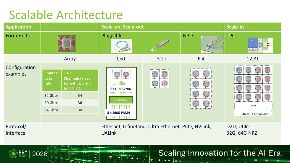
▲ Lumentum builds 1.6T and 3.2T pluggables, 6.4T NPO and 12.8T CPO from the same 1060 nm VCSEL array, and lists the number of spare channels at different lane rates (Image source: Lumentum | 2026 OCP Global Summit presentation)
Capacity | Form factor | Arrays (Tx+Rx) | Application | Electrical interface |
1.6T | Pluggable | 2 | Scale-up / Scale-out | 8x200G PAM4 via gearbox to 32x50G NRZ |
3.2T | Pluggable | 4 | Scale-up / Scale-out | Ethernet, InfiniBand, UEC, PCIe, NVLink, UALink |
6.4T | NPO | 8 | Scale-up / Scale-out | Same as above |
12.8T | CPO | 16 | Scale-in | D2D, UCIe, 32G / 64G NRZ |
Array counts are STT's count from the slide diagrams. The 12.8T chiplet uses 8 transmit and 8 receive arrays, about 4 mm wide, and the slide states "> 6 Tbps/mm". STT calculation: at 1.6T per array, 16 arrays total 25.6 Tb/s (12.8T each way); divided by 4 mm that is about 6.4 Tb/s/mm, matching the slide. Counting one direction only gives 3.2 Tb/s/mm. The most reasonable reading is that the density counts Tx and Rx together, but the slide does not state its basis.

▲ Going from 1.6T to 12.8T only raises the array count from 2 to 16; the 1.6T pluggable example needs a gearbox to convert PAM4 to NRZ, while the 12.8T scale-in configuration is natively NRZ on the electrical side (Image source: Simple Tech Trend original; data from Lumentum, 2026 OCP Global Summit presentation)
Look closely at the electrical interface row. The 1.6T pluggable goes through a gearbox that splits the switch's 8 lanes of 200G PAM4 into 32 lanes of 50G NRZ for the VCSELs, while the 12.8T scale-in chiplet takes 32G or 64G NRZ directly from D2D / UCIe with no conversion. Slow-and-wide saves energy because optics and electronics both run slow with no DSP; insert a gearbox and part of the saving is eaten. The slides give no power figure for that gearbox.
4. Breaking Down Sparing: Faster Lanes Cost More Spares
The easiest cell to miss is the small one on the left: how many channels a 1.6T array needs, including spares, to reach FIT below 1. The slide gives 54 at 32G, 36 at 50G and 30 at 64G.
STT splits that into required channels and spares:
Lane rate | Channels needed for 1.6T | Channels with spares | Spares | Spare ratio |
32 Gbps | 50 | 54 | 4 | 8% |
50 Gbps | 32 | 36 | 4 | 12.5% |
64 Gbps | 25 | 30 | 5 | 20% |
Required channels are 1.6T divided by lane rate; spares and ratios are STT calculations.

▲ Raising the lane rate from 32G to 64G cuts the required channels from 50 to 25 but raises the sparing ratio from 8% to 20%; bandwidth density goes from about 1 Tb/s/mm today to more than 6 Tb/s/mm in the 12.8T configuration, roughly a 6x gap on a like-for-like basis (Image source: Simple Tech Trend original; data from Lumentum, 2026 OCP Global Summit presentation)
The numbers say one thing: faster lanes mean fewer channels, but each channel needs more backup. The speaker did not explain why. STT's inference: the channel count halves while the spare count does not fall, which suggests per-element failure rates rise at higher speed (higher current density and stress), so proportionally more spares are needed to bring the array back to FIT below 1. Slow-and-wide reliability, in other words, comes not from VCSELs that never fail, but from building a few extra into every array.
5. Where Is the Evidence: A 1 Tb/s/mm PCIe 5 Demo
On packaging, Lumentum showed two ways to integrate with CMOS:
Wafer-level fan-out package (WLFOP): standard VCSEL, PD, driver and TIA dies are molded into one plane, a redistribution layer (RDL) is plated on the back, and a heat spreader goes on top. The speaker said this technology won an award at ECOC three weeks earlier.
3D stacking: PDs and VCSELs are bumped directly onto an ASIC containing the PHY, TIA, CDR and driver.

▲ Lumentum's two CMOS integration approaches: wafer-level fan-out packaging (WLFOP) and VCSEL/PD 3D stacking on the ASIC (Image source: Lumentum | 2026 OCP Global Summit presentation)
Because each element runs at 32 to 64G, array pitch does not need to be aggressive, and Shchekin stressed that copper pillar or thermocompression bonding is enough; hybrid bonding is not required.
The hardware you can verify is an optical PCIe demo with Astera Labs and Corning:
1060 nm 3D FOWLP VCSEL / PD transmit and receive optical engines, paired with Astera Labs Scorpio PCIe switches in the same NPO / CPO-like rack tray
Multiple 32 Gb/s NRZ channels running error-free PCIe 5.0 over Corning OM3 multimode fiber; the solution targets tens of meters over multimode fiber
Bandwidth density of about 1 Tb/s/mm today, with about 4 Tb/s/mm in sight; the optical engine has a path to below 2.5 pJ/bit (the slide says "path to", so this is a target)

▲ The Lumentum, Astera Labs and Corning optical PCIe rack-scale demo: 1060 nm VCSEL/PD optical engines, a Scorpio PCIe switch and OM3 multimode fiber (Image source: Lumentum | 2026 OCP Global Summit presentation)
Put it next to the table in section 3: the demo is 1 Tb/s/mm at 32G, the 12.8T configuration is above 6 Tb/s/mm at 64G. If both use the same density basis, that is a gap of about 6x, and Lumentum's own stated next step is 4 Tb/s/mm.
6. Risks and Counterarguments
12.8T is a configuration example, not a product. The slides give no schedule and no power or yield figures for 12.8T; what can be verified today is a PCIe 5-class demo.
Gearbox power is not disclosed. Ethernet pluggables need PAM4-to-NRZ conversion, and the power and latency of that chip are not public, so the efficiency case for this column cannot be checked.
pJ/bit has no common boundary. Below 2.5 pJ/bit is a target path for the optical engine, not a measurement, and it covers the engine only; Lumentum's own call to action asks the industry to define the system boundary, which means vendors' numbers cannot be compared directly today.
Fiber count is still a challenge. STT estimate: at 64G, 12.8T means about 200 active lanes each way; at one fiber per lane, one chiplet needs about 400 fibers. NVIDIA's ECOC VCSEL review also pointed to fiber as the main bottleneck for slow-and-wide; see ECOC2026 | VCSELs Already Hit ≤1 pJ/bit; Fiber Is What Holds Them Back. "Existing fiber and connector ecosystem" refers to components, not fiber count.
Density still trails hyperscaler targets. Microsoft's optical I/O target at ECOC is above 10 Tbps/mm (see ECOC2026 | Microsoft Wrote Down the Spec Sheet for Optical I/O); Lumentum's 12.8T configuration is about 60% of that and today's solution about one tenth. Density bases (one direction or Tx+Rx) differ by company, so treat this as an order-of-magnitude comparison.
7. What It Means for Taiwan's Supply Chain
The talk named no Taiwanese companies. The only partners named were Astera Labs (PCIe switch) and Corning (multimode fiber), and Lumentum has its own VCSEL production.
"Reusing the 3D sensing supply chain" is the most direct signal for Taiwan's GaAs industry. Taiwan has volume experience in GaAs epitaxy and foundry for 3D sensing VCSELs; but the "3D sensing supply chain" in this talk refers to Lumentum's own volume platform, no outside foundry was mentioned, and 1060 nm epitaxial structures differ from 850 nm. Whether Taiwanese suppliers can enter depends on whether Lumentum opens outside capacity, and there is no public information on that.
The packaging route is friendly to Taiwan's OSATs. Wafer-level fan-out, copper pillar and thermocompression bonding are mature processes in Taiwan's packaging industry; by avoiding hybrid bonding, Lumentum puts the bar where a typical OSAT can reach it. Worth watching is who wins WLFOP optical engine assembly.
Multimode fiber and connectors depend on fiber count. If slow-and-wide really scales to hundreds of fibers per chiplet, high-count multimode jumpers and connector assembly become new value, but the talk gave no detail on fiber architecture.
8. Conclusion
Lumentum's slow-and-wide strategy is clear: instead of chasing the fastest single lane, it turns one 1060 nm flip-chip VCSEL array into a building block, trading array count for bandwidth, spares for reliability and existing packaging for volume. 12.8T is simply the same array 16 times.
Separate the timelines. What can be verified today is a PCIe 5, 32G, roughly 1 Tb/s/mm demo; 4 Tb/s/mm is Lumentum's stated next step; a 12.8T scale-in CPO above 6 Tb/s/mm is still a configuration drawing. Our view is that the first volume landing for slow-and-wide VCSELs will be PCIe optical interconnect, which is natively NRZ on the electrical side and already demonstrated in hardware, not Ethernet pluggables that need a gearbox; scale-in has the best-fit electrical interface but must wait for 64G NRZ and the 12.8T chiplet, so it comes after PCIe. If we are wrong, the signal will be Lumentum announcing a 1.6T pluggable customer and gearbox power first. Three things to watch over the next 12 months: when a 64G NRZ, roughly 4 Tb/s/mm optical engine shows measured data; whether gearbox power for the pluggable version is disclosed; and when a pJ/bit definition with a consistent system boundary takes shape.
Slow-and-wide is not won by the fastest VCSEL, but by whoever can copy the same array the most times with the most ordinary packaging.
This article is for technology and industry trend analysis only and does not constitute investment advice.


Comments