


ECOC 2026 | VCSELs Hit ≤1 pJ/bit Long Ago; Fiber Is the Real Bottleneck. Did NVIDIA Pause Its Slow-and-Wide Project Over It, and Propose a New 26/80 Fiber?
NVIDIA's Daniel Kuchta delivered a panoramic review of VCSELs, and one line on his conclusion slide set the tone for the whole talk: "≤1 pJ/bit all-in has been demonstrated by multiple companies; it will be hard for other technologies to beat." Note the word "all-in": this is an end-to-end figure including drivers, TIAs and everything else. At the same conference, Microsoft set its in-rack optical I/O threshold at <1 pJ/bit. In other words, on power, VCSELs are already at the finish line. But the real message of the talk lay in two other sections: 200G is probably the last generation today's oxide-confined structure can squeeze out; and what blocks scaling is not the laser but the fiber and connectors. NVIDIA's own slow-and-wide research project was paused precisely because fiber cost too much. So the speaker did something rare on stage: he publicly proposed a new fiber spec, with a 26 µm core, 80 µm glass, 1060 nm operation and an EMB of about 5 GHz.
1. Why VCSELs Are Still on the Table: One Line Settles the Debate
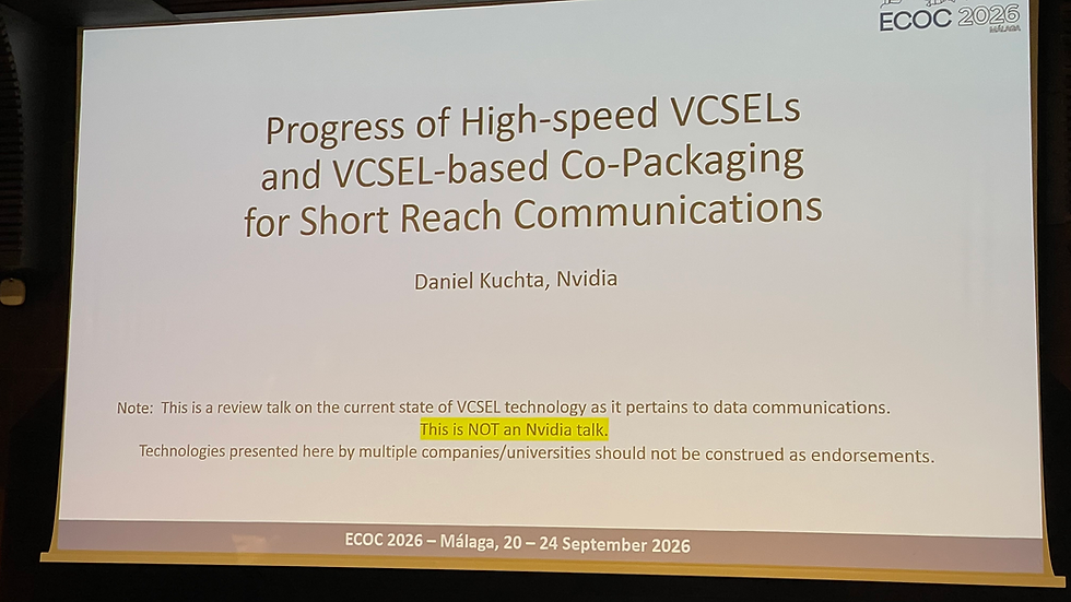
First, the framing. The speaker opened by stating that this was a survey covering technologies from many companies and did not represent an NVIDIA endorsement of any of them.
The slide listed seven VCSEL advantages: the lowest energy per bit, the lowest cost per channel, easy high-density parallel arrays (with spare lanes for redundancy), simple coupling to multimode fiber, high-volume manufacturing across diverse supply chains, wafer-level test and burn-in, and error-free, low-latency NRZ operation.
And one line on the summary slide is the thing to remember from this talk:
≤1 pJ/bit all-in has been demonstrated by multiple companies; it will be hard for other technologies to beat.
Put that in the context of ECOC 2026 and it gets interesting. At the same conference, Microsoft set its in-rack optical I/O power threshold at <1 pJ/bit, and its bet is on microLED. But Kuchta's slide says: VCSELs have that number today, and not from just one company.
This does not mean VCSELs have won. It means that if pJ/bit were the only column on your scorecard, the race would already be over, so the real battlefield must lie elsewhere. The remaining forty minutes of the talk were about that "elsewhere."
2. Speed Records Keep Falling, but Check Whether BER Was Reported
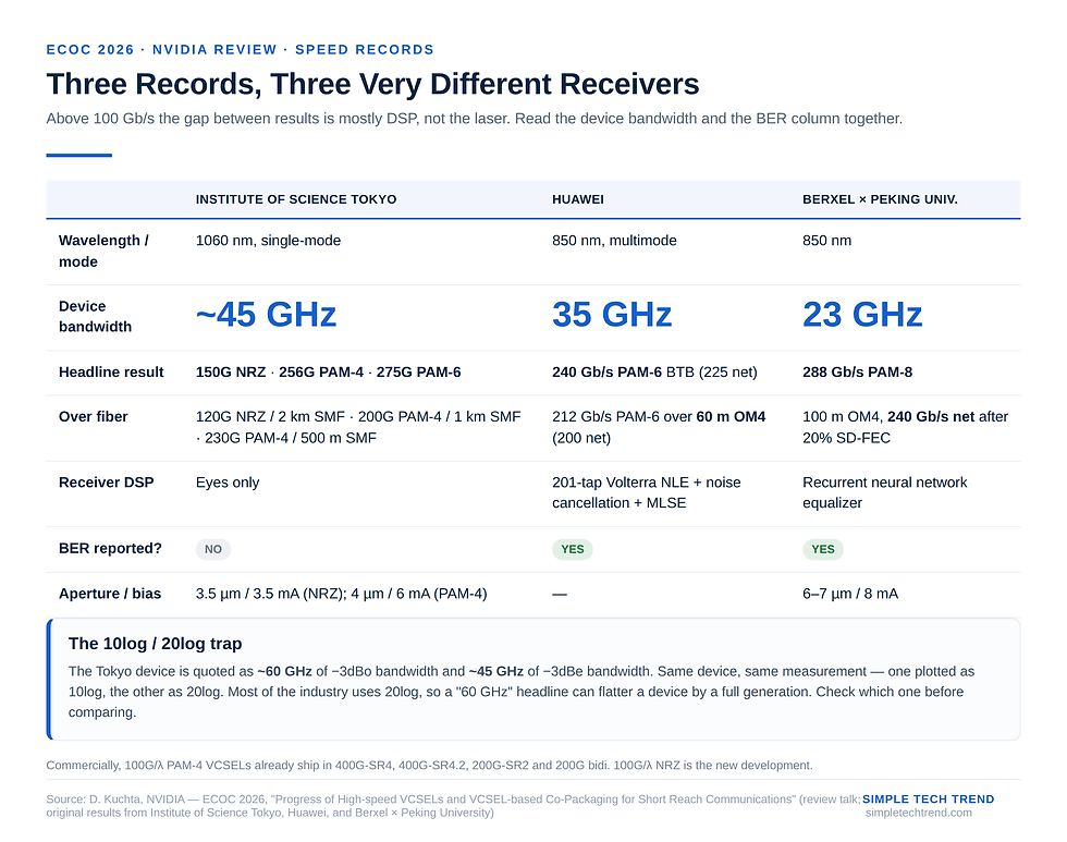
Progress in high-speed VCSEL literature was plotted on one chart: post-FEC data rate on the x-axis and fiber length on the y-axis. Every point beyond 200 m is on single-mode fiber. 100G/λ PAM-4 is already commercial, used in 400G-SR4, 400G-SR4.2, 200G-SR2 and 200G bidi; 100G/λ NRZ is a newer development.
Three records are worth writing down, but they should be read separately:
Institute of Science Tokyo (1060 nm single-mode VCSEL, back-to-back, eye diagrams only)
150G NRZ: ER 1.8 dB, 3.5 µm oxide aperture, 3.5 mA bias
256G PAM-4: ER 2.2 dB, TDECQ about 5 dB, 4 µm oxide aperture, 6 mA bias
275G PAM-6
Also achieved: 120G NRZ over 2 km of single-mode fiber, 200G PAM-4 over 1 km of single-mode fiber, and 230G PAM-4 over 500 m of single-mode fiber
The device bandwidth labeling deserves attention: the slide lists both a −3dBo bandwidth of about 60 GHz and a −3dBe bandwidth of about 45 GHz. These describe the same thing for the same device, one using 10log and the other 20log. The speaker called this out on stage because most of the industry uses 20log: when you see 60 GHz, check which one it is, or you will overestimate by a full generation. The box in the upper-right corner of the slide was also candid: "No BER reported."
Huawei (850 nm multimode VCSEL, 35 GHz bandwidth, BER reported)
240 Gb/s PAM-6 back-to-back, 225 Gb/s net
212 Gb/s PAM-6 over 60 m of OM4, 200 Gb/s net
The receiver used a 201-tap Volterra nonlinear equalizer + noise cancellation + MLSE
Berxel × Peking University (850 nm, PAM-8 record of 288 Gb/s)
The device has only 23 GHz of bandwidth, a 6–7 µm oxide aperture and 8 mA bias
Over 100 m of OM4, with recurrent neural network (RNN) equalization at the receiver
240 Gb/s net after 20% soft-decision FEC
Put the three side by side and the message is clear: most of the difference between records lies in the DSP, not the laser. Berxel's 23 GHz device reaches 288 Gb/s thanks to a neural-network equalizer; Huawei's 35 GHz device relies on a 201-tap Volterra. That is exactly the cost of the "fast-and-narrow" path, and much of this generation's pJ/bit debate is about whether that DSP should be counted. We unpacked this accounting question in ECOC 2026 | Three Hours of Fast-Narrow vs. Slow-Wide, and No One Defined "Slow": The Real Dividing Line Is 448G.
3. The Truth About Commercial 200G VCSELs: Great Records, No Product Yet
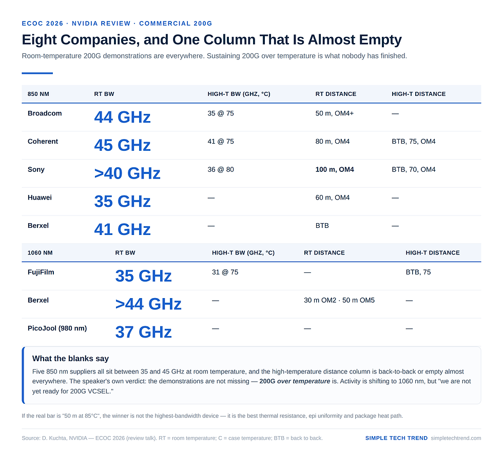
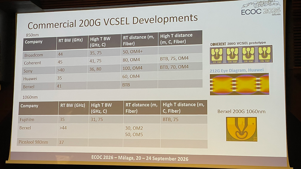
This is, in my view, the most valuable table of the talk for the supply chain. The speaker split companies developing 200G VCSELs into two groups by wavelength and listed four columns: room-temperature bandwidth, high-temperature bandwidth, room-temperature reach and high-temperature reach.
The 850 nm camp (five companies)
Broadcom: RT bandwidth 44 GHz; HT bandwidth 35 @ 75°C; RT reach 50 m, OM4+; HT reach —
Coherent: RT bandwidth 45 GHz; HT bandwidth 41 @ 75°C; RT reach 80 m, OM4; HT reach BTB @ 75°C, OM4
Sony: RT bandwidth >40 GHz; HT bandwidth 36 @ 80°C; RT reach 100 m, OM4; HT reach BTB @ 70°C, OM4
Huawei: RT bandwidth 35 GHz; HT bandwidth —; RT reach 60 m, OM4; HT reach —
Berxel: RT bandwidth 41 GHz; HT bandwidth —; RT reach back-to-back; HT reach —
The 1060 nm camp (three companies)
FujiFilm: RT bandwidth 35 GHz; HT bandwidth 31 @ 75°C; RT reach back-to-back @ 75°C
Berxel: RT bandwidth >44 GHz; HT bandwidth —; RT reach 30 m OM2 / 50 m OM5
PicoJool (980 nm): RT bandwidth 37 GHz; HT bandwidth —; RT reach —
What matters most in this table are the blank cells. On the 850 nm side, all five companies have room-temperature devices with bandwidths between 35 and 45 GHz, but the "high-temperature reach" column is almost entirely back-to-back or empty. The speaker was blunt: there is no shortage of room-temperature demos; what is missing is "200G support across temperature."
The 1060 nm side has fewer players, but activity is rising. Berxel's 1060 nm device already exceeds 44 GHz at room temperature and has run 30 m of OM2 and 50 m of OM5. The speaker's own view: "I don't know when 200G VCSELs will be commercialized. Activity is mainly moving on the 1060 nm side, so we may see it there first. But even with these demonstrations, we're not ready yet."
For Taiwanese suppliers, those blank cells are both an opportunity and a warning. If the real bar for 200G VCSELs is "still running 50 m at 85°C," the winner will not be the one with the highest bandwidth but the one with the best thermal resistance management, epitaxial uniformity and package heat dissipation. This is a contest of manufacturing and materials, not device physics.
4. VCSEL CPO/NPO Hardware You Can Already Touch
This section overturns a common assumption: many people think CPO equals silicon photonics. In fact, there are already several measurable physical VCSEL-based CPO and NPO implementations.
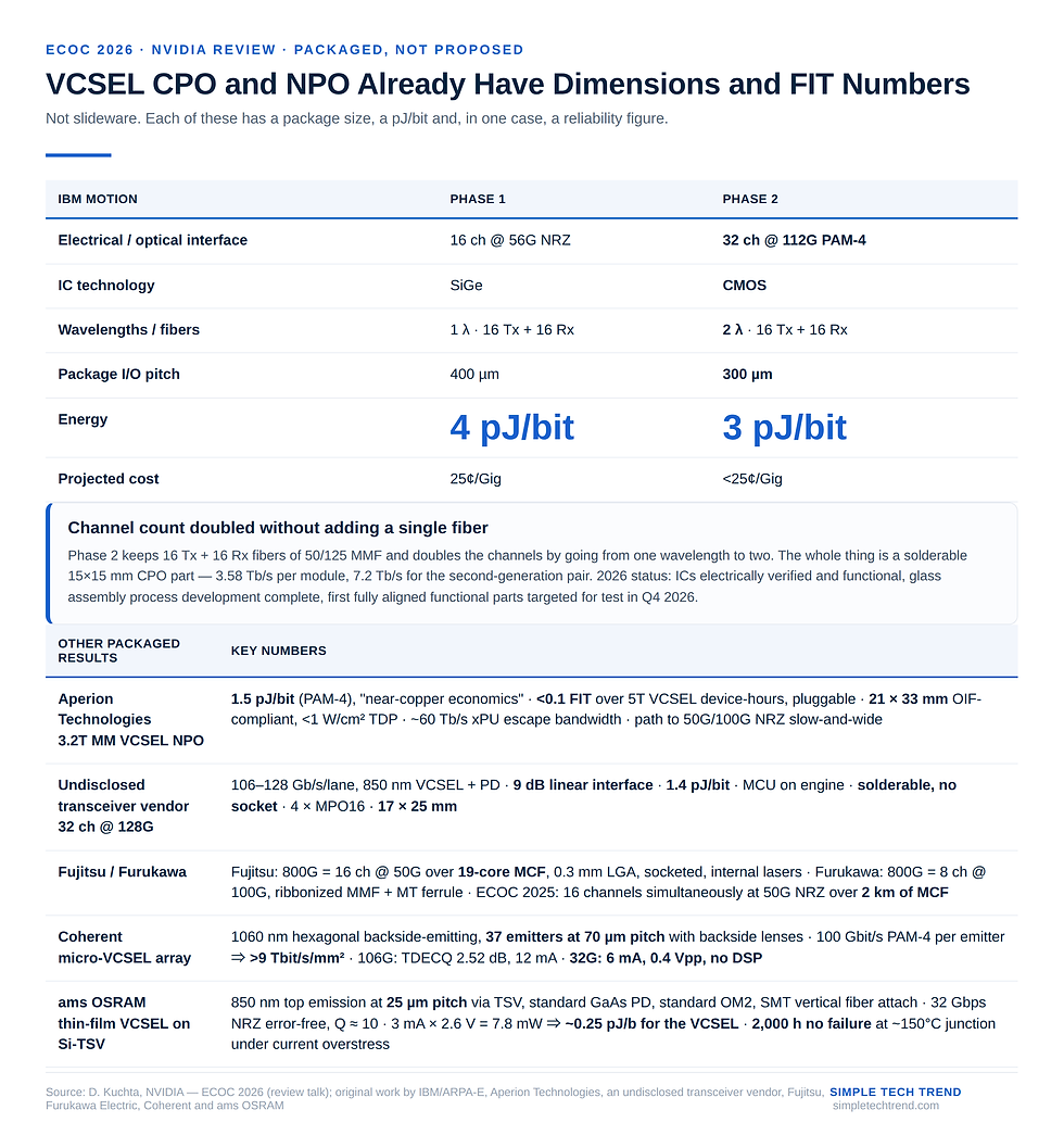
IBM MOTION (ARPA-E program) is a project the speaker worked on himself at IBM, and this time he gave a full two-generation comparison:
Electrical interface: Phase 1 is 16 channels @ 56G NRZ; Phase 2 is 32 channels @ 112G PAM-4
IC process: Phase 1 is SiGe; Phase 2 is CMOS
Number of wavelengths: Phase 1 is 1; Phase 2 is 2
Fiber count and type: both generations use 16 Tx + 16 Rx, 50/125 MMF
Package I/O pitch: Phase 1 is 400 µm; Phase 2 is 300 µm; the glass carrier is 13×13 mm in both generations
Energy: Phase 1 is 4 pJ/bit; Phase 2 is 3 pJ/bit
Estimated cost and interface: Phase 1 is 25 cents/Gig, Phase 2 under 25 cents/Gig; both use solder or LGA
Note that fiber count stays the same while channel count doubles, achieved by going from one wavelength to two. The whole device is 32 channels @ 112G PAM-4 packed into a 15×15 mm solderable CPO solution, or 3.58 Tb/s. The Phase 1 module was 1.8 Tb/s; two second-generation devices together reach 7.2 Tb/s.
The 2026 status was also specific: all subassemblies have been fabricated, the transceiver ICs have passed electrical testing and are functional, the glass assembly process has been developed, IC/VCSEL/PD assembly is under way, and the first fully aligned functional parts are expected to be testable in Q4 2026.
Aperion Technologies' 3.2T multimode VCSEL NPO package provided some of the hardest numbers of the talk:
Energy efficiency of 1.5 pJ/bit (PAM-4); the slide's own words: "approaching copper economics"
Reliability of <0.1 FIT, based on 5 trillion VCSEL device-hours, in a pluggable architecture
A 21 × 33 mm OIF-compatible package with TDP <1 W/cm²
About 60 Tb/s of xPU escape bandwidth
Scaling path: a slow-and-wide architecture at 50G/100G NRZ, moving toward integration into a single optical connector
There was also an unnamed transceiver vendor: 32 channels, 106–128 Gb/s per lane, 850 nm VCSEL + PD, 9 dB linear interface, 1.4 pJ/bit, an on-engine MCU, solderable (no socket), 4 × MPO16 optical interfaces, and 17 × 25 mm.
Together these three show one thing: VCSEL CPO/NPO is not a slideware concept; it already comes with dimensions, pJ/bit figures and FIT numbers. And the 1.4 to 1.5 pJ/bit range sits right between the <5 pJ/bit that silicon photonics CPO currently claims and Microsoft's <1 pJ/bit target.
Two Japanese vendors are moving in the same direction: Fujitsu uses 19-core multicore fiber, 800G = 16 channels @ 50G, 0.3 mm pitch LGA, socketed, with built-in lasers and a vertical connector; Furukawa uses ribbon multimode fiber, 800G = 8 channels @ 100G, with MT ferrules and a microlens array. An ECOC 2025 paper already demonstrated 16 channels running simultaneously at 50G NRZ over 2 km of multicore fiber.
5. The Proposal: A New 26/80 Fiber
This is the most opinionated part of the talk, and the part I think Taiwan's fiber and connector supply chain most needs to see.
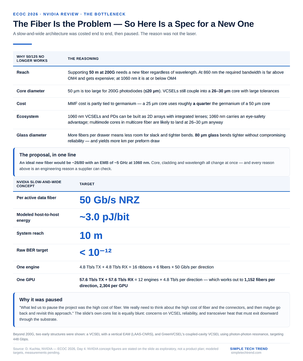
The starting point is simple: to run 50 m at 200G, a new fiber is needed regardless of wavelength.
At 860 nm, the required fiber bandwidth is far higher than OM4, which makes the fiber more expensive
At 1060 nm, because dispersion is much lower, the required fiber bandwidth is lower than or equal to OM4
The speaker's reasoning: since new fibers like OM5 are already expensive, rather than piling ever-higher-bandwidth fiber onto 850 nm, moving to 1060 nm can actually yield a cheaper fiber.
But he then said "that's not enough," and listed reasons to shrink the core as well:
A 50/125 µm core is too large and mismatched to 200G photodetectors (≤20 µm)
VCSELs can still couple into a 26–30 µm core with generous tolerance
Part of multimode fiber cost is tied to germanium, so a smaller core should be cheaper (a 25 µm core uses only a quarter of the germanium of a 50 µm core)
1060 nm VCSELs and PDs can be built as 2D arrays with integrated lenses, and 1060 nm has an eye-safety advantage
The multimode cores of multicore fibers are likely to fall in the 26–30 µm range anyway
Then he said "still not enough" and cut the glass diameter too:
A 125 µm glass diameter is too large
More fibers per drawer means less room for slack and tighter bend radii
80 µm glass can bend more tightly without sacrificing reliability
With 80 µm glass, the same preform can be drawn into more kilometers of fiber
The conclusion line was very specific:
The ideal new fiber should be roughly 26/80, with an EMB of about 5 GHz at 1060 nm.
This proposal is being pushed in the IEEE community, and it changes three things at once: core diameter, glass diameter and wavelength. For Taiwan's fiber, connector and passive component makers, this is a rare window where "the spec isn't set, but the demand has been stated publicly," and the one stating it is NVIDIA.
6. Slow-and-Wide by the Numbers: 57.6 Tb/s per GPU, and Then the Project Was Paused
This is the most candid part of the talk, and one of the few cases at ECOC 2026 where someone said publicly, "We ran the numbers, and then we stopped."
First, NVIDIA Research's slow-and-wide concept design. The numbers are all on the slide:
Per active data fiber: 50 Gb/s NRZ
Simulated end-to-end energy efficiency: about 3.0 pJ/bit (host-to-host)
System reach target: 10 m
Raw BER target: <10⁻¹²
The architecture is lensed VCSEL and PD chips forming a CMOS optical backplane, plus vertical fiber connectors. Capacity stacks up like this:
One engine: 4.8 Tb/s TX + 4.8 Tb/s RX = 16 ribbons × 6 fibers × 50 Gb/s (per direction)
One GPU: 57.6 Tb/s TX + 57.6 Tb/s RX = 12 engines × 4.8 Tb/s (per direction)
Follow the math to the end: one GPU needs 1,152 fibers per direction, or 2,304 fibers in total. And the speaker mentioned on stage that they once ran the numbers for an entire data hall and arrived at a scale of 60,000 fibers.
Then he delivered the most important line of the talk: what made us pause this project was the high cost of fiber.
His exact words: "What really stopped us was the high cost of the fiber. We really need to rethink the cost of fiber and connectors, and then maybe come back and revisit this approach."
The slide titled "Future option: slow-and-wide VCSEL arrays" also laid out the pros and cons candidly: the pros are potential power and cost efficiency and simple communication channels; the cons are concerns over VCSEL reliability and the need to remove transceiver heat down through the substrate.
This section brings "slow-and-wide" down from the level of ideas to the level of the ledger. In After Copper Runs Out for AI: Seven Paths for Scale-Up Optical Interconnect and the Two Ways Each Hits a Wall we explained that fast-and-narrow and slow-and-wide each hit their own wall. NVIDIA's case puts a precise name on the slow-and-wide wall: the unit price of fiber and connectors.
Other players in the same section are also pushing for density, and they all gave hard numbers:
ams OSRAM: 850 nm thin-film VCSELs on silicon with TSVs; integration is complete. Dense 25 µm pitch, standard GaAs photodetectors, standard OM2 fiber, and vertical fiber attach using the SMT ecosystem. Error-free 32 Gbps NRZ operation, Q factor about 10, 3 mA × 2.6 V = 7.8 mW, or about 0.25 pJ/b (VCSEL only). Reliability modeling shows no failures after 2,000 hours at about 150°C junction temperature under current overstress.
Coherent: a hexagonal back-emitting micro-VCSEL array at 1060 nm, with 37 emitters at 70 µm pitch, including backside lenses. A single emitter can reach 100 Gbit/s (PAM-4), implying a bandwidth density of >9 Tbit/s/mm². At 106 Gbit/s: TDECQ 2.52 dB, 12 mA current, 7 taps each on Tx and Rx; at 32 Gbit/s: 6 mA current, 0.4 V Vpp, and no DSP at all.
Coherent's >9 Tbit/s/mm² deserves to be circled on its own. Compare it with Microsoft's >10 Tbps/mm target for optical I/O (linear shoreline density) and the 1.33 Tb/s/mm² of NVIDIA's microring test chip (areal density): on areal density, micro-VCSEL arrays currently lead.
7. Is There a Path Beyond 200G? Two Early-Stage Approaches
The speaker gave a clear verdict on the current structure: 200G will probably be the last data rate today's modulated oxide-confined structure can squeeze out. Going higher will require a new approach.
The slide offered two paths, both still at an early stage:
Path one: VCSEL + vertical EAM. From LAAS-CNRS, an electro-absorption modulator integrated vertically above the VCSEL; the slide's comment was that it "has high potential to reach higher bandwidth."
Path two: coupled-cavity VCSEL. GreenVCSEL, working with a major VCSEL supplier, uses a structure with a current-pumped active cavity on top, a DBR in the middle and a passive cavity below, exploiting photon-photon resonance for optically enhanced modulation. The target is 448 Gbps.
The 448 figure is not arbitrary. It lines up exactly with the most hotly debated line at this year's workshop: the fast-and-narrow camp's push to take a single lane to 448G. If coupled-cavity VCSELs really get there, the boundary between fast-and-narrow and slow-and-wide will be redrawn. The speaker's own words were restrained: "Our simulations show it should be able to support 448 Gbps. I wish them luck."
8. Conclusion
Placed on the map of ECOC 2026, this talk occupies a special position: in a conference where everyone was talking about silicon photonics and microLED, it was the only talk that stood up and said "VCSEL energy efficiency was solved long ago."
The speaker put it vividly: "Even though silicon photonics has sucked all the air out of the room, a lot of good things are still happening with VCSELs."
For Taiwan's supply chain, there are three concrete takeaways:
First, stop treating power as an open question for VCSELs. ≤1 pJ/bit all-in has been achieved by multiple companies; Aperion's 1.5 pJ/bit is for an entire 3.2T NPO package, while ams OSRAM's 0.25 pJ/b is for the VCSEL device itself. The three questions that actually matter now are: can it run 50 m at 85°C, can its reliability withstand co-packaging, and how much do the fiber and connectors cost.
Second, the 26/80 proposal is a rare public demand signal. It calls for shrinking the core from 50 to 26, the glass diameter from 125 to 80, and shifting the wavelength from 850 to 1060, all for verifiable engineering reasons: PD size, germanium usage, bend reliability, preform draw length and eye safety. For fiber and connector makers, this is order demand that hasn't been standardized yet but whose spec NVIDIA has already stated publicly. It also opens opportunities in 1060 nm PDs, lens arrays and MT/multicore ferrules.
Third, and most important as a warning: NVIDIA ran the numbers on slow-and-wide and paused because of fiber cost. At 2,304 fibers per GPU and 60,000 per data hall, the unit price of fiber and connectors decides whether the whole architecture succeeds. That is both bad and good news for Taiwanese suppliers: the bad news is that slow-and-wide will land later than people expect; the good news is that whoever makes that 26/80 fiber and its matching connectors cheap enough will be the one who unlocks this path.
Verdict: The most valuable thing about this talk is not any single technical advance; it formally shifts the focus of VCSEL competition from "fast enough and power-efficient enough" to "are the fiber and connectors cheap enough." When a GPU company runs the numbers on its own slow-and-wide architecture, hits pause because of fiber cost, and then proposes a new fiber spec on stage, this is no longer a component-level discussion. The next step for VCSELs is not in the epi fab; it is in the draw tower and the ferrule molds.
This article is for technology and industry trend analysis only and does not constitute investment advice.
Related Reading
ECOC 2026 | Three Hours of Fast-Narrow vs. Slow-Wide, and No One Defined "Slow": The Real Dividing Line Is 448G: why 448G is the dividing line, and why pJ/bit accounting can differ by 54x
ECOC 2026 | Data Centers Need Billions of Lasers, but the Bottleneck Is the 5 Minutes It Takes to Attach Them: the capacity bottleneck for light sources is not emission but packaging and alignment, the other side of this article's "fiber is the bottleneck" story
After Copper Runs Out for AI: Seven Paths for Scale-Up Optical Interconnect and the Two Ways Each Hits a Wall: the walls that fast-and-narrow and slow-and-wide each hit, and how the seven approaches coexist in layers



Comments