


ECOC 2026 | 850nm Dies at 1,600 Hours, 1060nm Hits 5,000 Hours with Zero Failures: How One Lumentum Chart Moved the VCSEL Battle from Speed to Heat
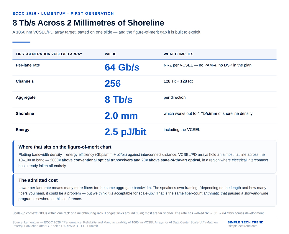
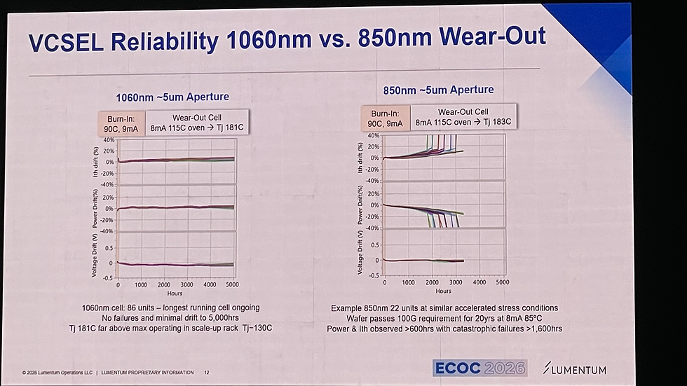
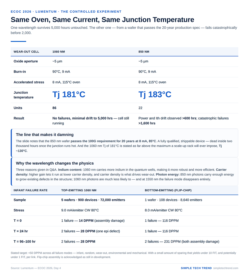
Only one slide in this talk really matters, and it isn't about speed. Lumentum ran a remarkably clean controlled experiment—the same ~5 µm aperture, the same burn-in, the same 8 mA in a 115°C oven, with junction temperatures of 181–183°C, 1060 nm on the left and 850 nm on the right. The result: all 86 of the 1060 nm devices reached 5,000 hours with no failures and minimal drift; the 22 850 nm devices began showing power and threshold-current drift at 600 hours and catastrophic failures after 1,600 hours. And the slide makes a point of noting: that 850 nm wafer passed the "8 mA, 85°C, 20-year, 100G" production spec. In other words, a qualified 850 nm device simply cannot survive the thermal environment of a scale-up rack—while 1060 nm came through unscathed at a 181°C junction temperature (far above the actual in-rack Tj ~130°C). That is why Lumentum sees 1060 nm as the answer for scale-up, and its Gen 1 spec is: 64 Gb/s NRZ × 256 channels = 8 Tb/s, 2.0 mm shoreline, 2.5 pJ/bit.

1. Gen 1 Specs: 8 Tb/s Squeezed into 2 mm of Shoreline
First, the goal. This talk is about scale-up—connecting GPUs within the same rack or adjacent racks, up to about 30 meters, and usually much shorter.
The speaker positioned the technology with a figure-of-merit chart: interconnect distance on the x-axis and "bandwidth density × energy efficiency (Gbps/mm ÷ pJ/bit)" on the y-axis. The chart is split into three regions—In-Package, On Board, and Off Board—with four curves:
Electrical interconnect: falls steadily and is uncompetitive beyond one meter
State-of-Art Optical: flatter than electrical, but falls short beyond 10 meters
Conventional optical transceivers: the entire curve hugs the bottom
VCSEL/PD arrays: a nearly flat line that, in the 10–100 m range, is 2000× higher than conventional transceivers and 20× higher than state-of-art optical
The "Gen 1" annotation in the lower-right corner is very specific:
VCSEL/PD array Gen 1: 64 Gb/s NRZ per VCSEL × 256 channels (8 Tb/s), 2.0 mm shoreline, 2.5 pJ/bit
Do the math and its position becomes clear: 8 Tb/s ÷ 2.0 mm = 4 Tb/s/mm of shoreline density. Compare that with 0.8 Tb/s/mm for NVIDIA's microring test chip and the 0.3 T/mm Huawei set for its 1024-lane switch—VCSEL arrays lead on shoreline density, and they do it with plain NRZ.
The 2.5 pJ/bit figure also needs context: it is a link-level number that includes the VCSEL—higher than Aperion's 1.5 pJ/bit at the same conference, but well below the <5 pJ/bit claimed for silicon photonics CPO.
The speaker also acknowledged the biggest controversy around the VCSEL approach: cost. Because the per-channel rate is low, the same aggregate bandwidth requires many more fibers. His take was pragmatic: "Depending on the distance and how many fibers you need, this could be an issue—but we think it is acceptable for scale-up."
That line is worth remembering, because it is exactly the reason NVIDIA gave in its retrospective talk the same day for pausing its slow-and-wide project. We cover the full context in After Copper Can't Keep Up with AI: Seven Paths for Scale-Up Optical Interconnect and Two Ways to Live with Their Walls.
2. Why Back-Side Emission plus Flip-Chip: Thermal Resistance Down 40%
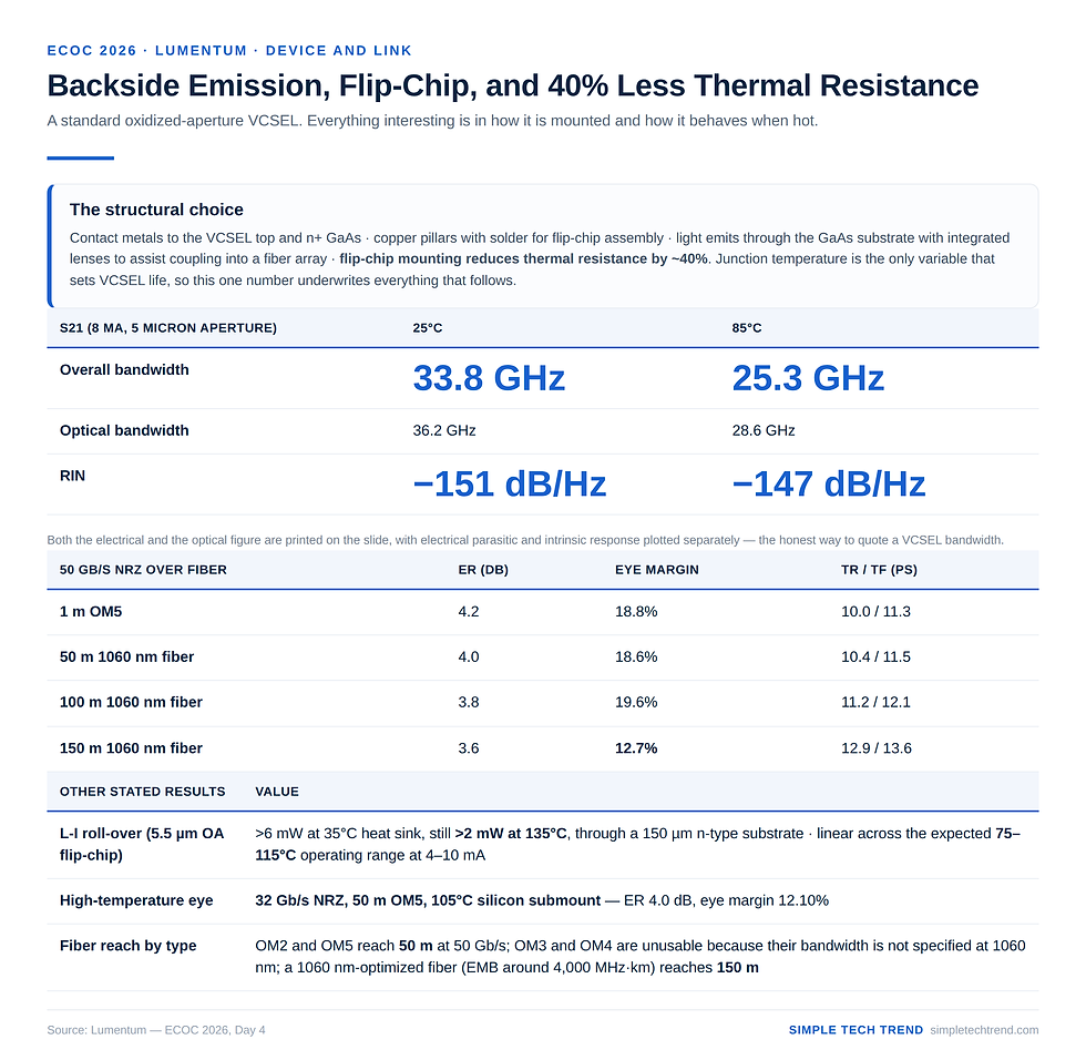
The device structure itself has no tricks—a standard VCSEL structure with an oxide aperture. The real design choice lies in the packaging:
Contact metal to the VCSEL top and the n+ GaAs
Copper pillars with solder for flip-chip assembly
Light exits through the back of the GaAs substrate, with an integrated lens on the substrate to aid coupling into the fiber array
And the key conclusion: flip-chip VCSELs cut thermal resistance by about 40%.
This is the physical foundation of the entire talk. Back-side emission (BSE) plus flip-chip places the heat-generating active region directly against the heat-sinking submount rather than on the far side of the whole chip. A 40% reduction in thermal resistance means a much lower junction temperature at the same bias current—and junction temperature is the single variable that determines VCSEL lifetime.
The LI curves confirm it. For a 5.5 µm-aperture flip-chip 1060 nm VCSEL, across eight curves from a heatsink temperature of 35°C up to 135°C:
Output power exceeds 6 mW at 35°C
Peak power still exceeds 2 mW at 135°C
The slide notes: power and rollover point are much higher than for top-emitting VCSELs of the same aperture size, because of the poorer heat conduction of top emitters
Highly linear across the expected 75–115°C operating range, at 4 to 10 mA depending on data rate
And this is power measured after passing through 150 µm of n-type substrate—in the speaker's words, "plenty of power even through the substrate."
3. Performance: 33.8 GHz, −151 dB/Hz, and Only an ~8 GHz Drop at 85°C
The S21 measurements give four numbers, at both 25°C and 85°C:
25°C: overall bandwidth 33.8 GHz; optical bandwidth 36.2 GHz; RIN −151 dB/Hz
85°C: overall bandwidth 25.3 GHz; optical bandwidth 28.6 GHz; RIN −147 dB/Hz
(8 mA bias, ~5 µm aperture)
Two things stand out here.
First, the slide gives both "overall bandwidth" and "optical bandwidth," and plots the electrical parasitics separately from the intrinsic response. This is exactly the 10log/20log trap called out in NVIDIA's retrospective talk at the same conference—Lumentum labels both conventions, which is the honest approach.
Second, going from 25°C to 85°C costs only 8.5 GHz. Compare that with commercial 200G VCSELs today—most 850 nm devices drop to around 35 GHz at 75°C—and it is clear this temperature stability is 1060 nm's real selling point.
RIN matters too. −151 dB/Hz at 25°C and still −147 dB/Hz at 85°C; the speaker also noted that the device's S21 shows some overshoot, "not really suited to PAM-4—it's designed for NRZ". That is a clear strategic choice: compete on channel count, not on modulation format.
4. In Practice: 50G to 150 Meters, 32G at 105°C
The NRZ results come in two sets.
The reach set (50 Gb/s NRZ):
1 m OM5: ER 4.2 dB; eye margin 18.8%; rise/fall time 10.0 / 11.3 ps
50 m 1060nm fiber: ER 4.0 dB; eye margin 18.6%; rise/fall time 10.4 / 11.5 ps
100 m 1060nm fiber: ER 3.8 dB; eye margin 19.6%; rise/fall time 11.2 / 12.1 ps
150 m 1060nm fiber: ER 3.6 dB; eye margin 12.7%; rise/fall time 12.9 / 13.6 ps
The slide's conclusion has three lines: the first implementation is expected to use NRZ; 1060 nm VCSELs have demonstrated 50 Gb/s NRZ over 50 m of OM2 and OM5, and 150 m over 1060 nm-optimized fiber; flip-chip 1060 nm VCSELs have demonstrated 32 Gb/s at 105°C.
The 105°C high-temperature eye deserves a closer look: 32 Gb/s NRZ, 50 m OM5, silicon submount at 105°C, ER 4.0 dB, eye margin 12.10%. That means the submount is at 105°C and the active region is even hotter—already beyond the measurement conditions of most 850 nm devices.
On that "1060 nm-optimized fiber," an audience member asked during Q&A whether it is still multimode. The speaker's answer: it is basically ordinary OM fiber with a modified doping profile that moves the minimum-dispersion point to 1060 nm, with an EMB of around 4,000 MHz·km—"better than OM5 at 850 nm." But he also acknowledged: it is still a new fiber.
He ruled out OM3 and OM4 outright—their bandwidth simply isn't specified at 1060 nm. The only usable options are OM2 (originally optimized for 850 and 1300 nm) and OM5, and only out to 50 meters.
This is the same story as NVIDIA's proposal for a new 26/80 fiber at the same conference: the 1060 nm devices are ready; the fiber isn't. We cover the light source and packaging capacity bottlenecks in ECOC 2026 | Data Centers Need Billions of Lasers, but the Bottleneck Is the 5 Minutes It Takes to Attach Them.
Another point is very useful for system vendors: customers have asked to push pJ/bit even lower. The speaker's physical intuition: turn the current down and power falls roughly with the square of the current, while bandwidth falls slightly less than linearly—so the figure of merit improves. The low-power eye-diagram table on the slide proves it: across a 2.5 to 4.0 mA bias range, at 1 m and 30 m of OM2, at 25 and 32 Gb/s, and at 25°C and 85°C, the eyes remain open.
5. The Reliability Chart: The Real Conclusion of the Talk
In my view this is the single most convincing slide of ECOC 2026, because it is a fully matched controlled experiment.
Conditions for both groups:
Burn-in: 1060 nm (~5 µm aperture) 90°C, 9 mA; 850 nm (~5 µm aperture) 90°C, 9 mA
Accelerated conditions: 1060 nm (~5 µm aperture) 8 mA, 115°C oven; 850 nm (~5 µm aperture) 8 mA, 115°C oven
Junction temperature: 1060 nm (~5 µm aperture) Tj 181°C; 850 nm (~5 µm aperture) Tj 183°C
Sample size: 1060 nm (~5 µm aperture) 86 devices; 850 nm (~5 µm aperture) 22 devices
Results:
1060 nm: ran to 5,000 hours with no failures and minimal drift, and the cell is still running. The threshold-current, power, and voltage drift plots are all flat.
850 nm: power and threshold-current drift observed after 600 hours, with catastrophic failures after 1,600 hours. Those curves break off between 2,000 and 3,000 hours.
And the slide adds one critically important note on the 850 nm group: this wafer passed the "8 mA, 85°C, 20-year, 100G" specification.
In plain terms: a fully qualified, shippable 850 nm device, placed in the thermal environment of a scale-up rack, will fail in under two thousand hours. This is not a yield problem; it is a materials problem.
In Q&A, the speaker explained the physics on three levels:
1. Doping and gain: to raise gain, 850 nm needs a lot of indium in its quantum wells, whereas 1060 nm inherently has a higher indium content, which makes it more robust and more efficient.
2. Carrier density: 1060 nm has higher gain, so it can operate at a lower carrier density—and carrier density is the main driver of wear-out.
3. Photon energy: 850 nm photons carry enough energy to grow defects already present in the structure; 1060 nm photon energy is much lower and unlikely to drive that. He added a comparison: at 1550 nm the photon energy is too low, so this failure mode never shows up at all.
The final number is the decider: the slide states that Tj 181°C is far above the maximum operating temperature inside a scale-up rack, Tj ~130°C.
In other words, 1060 nm ran 5,000 hours unscathed under conditions far harsher than actual use. The extrapolation the speaker cited: under low-stress conditions, the model yields a mean time to failure on the order of 100,000 years.
6. Infant Mortality: 72,000 Emitters, 28 DPPM
With wear-out solved, next comes early failure. This is where Lumentum's real moat shows—its volume-production test infrastructure from 3D sensing.
Test scale for the top-emitting 1060 nm arrays:
5 wafers × 180 devices × 80 emitters = 900 devices, 72,000 emitters
Stress conditions: 9.0 mA/emitter, CW, 80°C
Readout conditions: 9.0 mA/emitter, 1.0 ms, 10% duty cycle, 25°C
Pass criterion: emitter power of 3 to 10 mW
T = 0 hr: 1 emitter failure (assembly damage); DPPM 14
T = 24 hr: 2 emitter failures (one new epitaxial defect); DPPM 28
T = 96 hr: 2 emitter failures; DPPM 28
Out of 72,000 emitters, only two failed after 96 hours of stress—and one of those was caused by assembly.
The bottom-emitting (flip-chip) group is still at an early stage: 1 wafer, 108 devices, 8,640 emitters; 1 failure at T=0 (116 DPPM) and 2 at T=100 hours (231 DPPM), and both were damaged during assembly. The slide candidly notes: the flip-chip assembly process is still in development, with more wafer data expected by year-end.
The end point of the whole reliability argument is on the same slide:
The target is <50 DPPM, covering every failure mode: infant mortality, random, wear-out, environmental, and mechanical.
The speaker then added the system-level translation: once that target is met, adding just a few spare channels can bring each link below 10 FIT, or even below 1 FIT.
This "redundancy for reliability" logic is fully consistent with Microsoft's argument for slow-and-wide at the same conference—when there are many channels, the marginal cost of a few extra is close to zero, so reliability is engineered through architecture, not by pushing a single device to the limit.
7. Manufacturing: Riding a Line That Has Already Shipped Billions
The final section covers what is hardest to replicate about this approach, and it has little to do with optical communications—it has to do with the iPhone's Face ID.
The slide lays it out clearly:
Based on 6-inch GaAs, with one pointed note: it sidesteps InP supply issues
Leverages the 3D sensing (3DS) VCSEL supply chain: billions of 3DS VCSEL arrays shipped, with wavelength, optical power, threshold current, beam uniformity, reliability, and cost all tightly controlled
Epitaxial growth process and design adapted from 940 nm 3DS, tuned for 1060 nm and high speed
Wafer processes and equipment are the same as or very similar to existing 3DS products, including the back-side emission process
Quality control plans carry over as well: epitaxial growth, fab metrology, visual inspection, and device testing
In Q&A, someone asked about yield and die per wafer. The speaker's answer: the largest 3D sensing die come out at about 10,000 per 6-inch wafer; 1060 nm die are smaller, perhaps 30,000 to 40,000 per wafer, with 50 to 100 emitters per die. The 6-inch wafer image on the slide is labeled ~1 mm² die.
As for the device design itself, the slide sends a very flexible signal: the 80-emitter hexagonal array can map to custom fiber bundles, fiber shuffles, or multicore fibers of various pitches, and flip-chip-on-silicon fan-out boards with lenses have already been built.
The demo section revealed two partners:
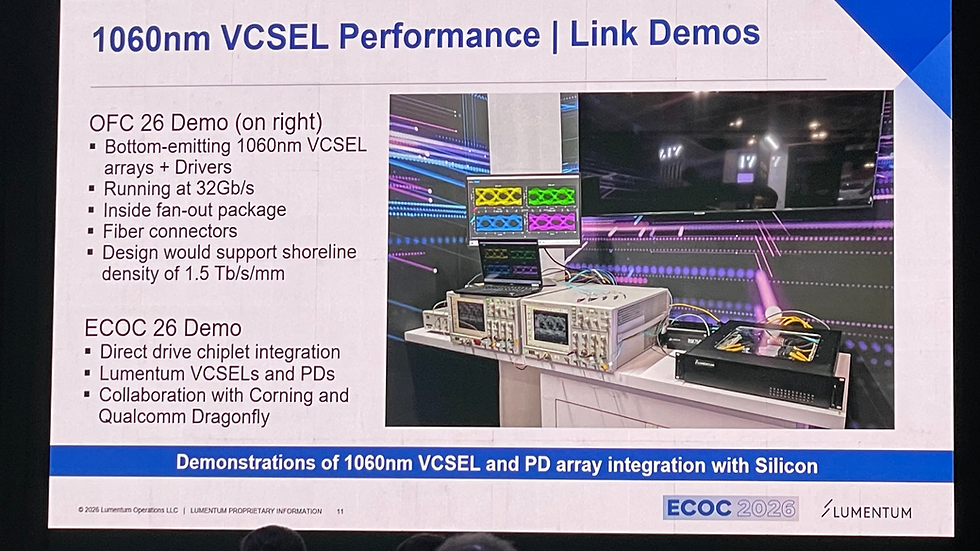
OFC 2026 demo: a bottom-emitting 1060 nm VCSEL array plus driver at 32 Gb/s, in a fan-out package with a fiber connector—a design that can support 1.5 Tb/s/mm of shoreline density
ECOC 2026 demo: direct-drive chiplet integration of Lumentum's VCSELs and PDs, in collaboration with Corning and Qualcomm Dragonfly
Qualcomm's appearance here is the easiest thing to miss in this talk—and the most telling. It shows that chiplet integration of 1060 nm VCSELs already has a major non-GPU player pushing behind it.
8. Conclusion
Placed in the context of ECOC 2026, this talk forms a complete narrative with NVIDIA's retrospective talk the same day: NVIDIA said VCSEL power consumption was solved long ago and that fiber is what's holding things back; Lumentum's talk answers the last open question—reliability.
For the Taiwan supply chain, three concrete takeaways:
First, the 850 vs 1060 comparison chart should become the standard question for evaluating any VCSEL solution. Stop asking "what is this device's bandwidth?" and ask instead "how many hours can it run at Tj 180°C?" Because an 850 nm wafer that passed a 20-year spec died in 1,600 hours under the same conditions—the 20 years on the datasheet were calculated at 85°C, and a scale-up rack is not that environment.
Second, 1060 nm's real barrier is not the device but that 3D sensing production line. 6-inch GaAs, 940 nm epi adapted to 1060 nm, volume statistics from billions of units, and a test methodology that can screen 72,000 emitters at once—none of this can be built by a newcomer within two years. For Taiwanese companies, the opportunity is not competing with Lumentum on VCSELs but supplying what it needs and doesn't make itself: fiber bundles, fiber shuffles, silicon fan-out submounts, lens arrays, and flip-chip assembly—note that it admits its flip-chip assembly process is "still in development," and nearly all current failures come from assembly.
Third, fiber remains the unsolved variable. OM3 and OM4 are unusable at 1060 nm, OM2 and OM5 only reach 50 meters, and the fiber that reaches 150 meters is a custom one that is "conceptually a simple change, but in practice a new product." Meanwhile, NVIDIA is proposing a new 26/80 spec at the same conference. Whoever first turns 1060 nm multimode fiber into a standard product will hold pricing power in this cycle.
Verdict: the most valuable thing in this talk is not the 8 Tb/s or the 2.5 pJ/bit; it is the chart that put 850 nm and 1060 nm in the same oven. It proves one thing: the VCSEL bottleneck in scale-up was never speed—it is heat, and heat is exactly what 1060 nm solves. When an 850 nm device that passed a 20-year spec fails within 1,600 hours while 1060 nm runs 5,000 hours unscathed at an even higher junction temperature, choosing a wavelength is no longer a matter of preference but of feasibility.
This article is for technology and industry trend analysis only and does not constitute investment advice.
Related Reading
After Copper Can't Keep Up with AI: Seven Paths for Scale-Up Optical Interconnect and Two Ways to Live with Their Walls: where VCSEL arrays sit among the seven scale-up approaches, and a full breakdown of the "many more fibers" cost
ECOC 2026 | Data Centers Need Billions of Lasers, but the Bottleneck Is the 5 Minutes It Takes to Attach Them: packaging and alignment bottlenecks from the same conference's light source workshop, corroborating the flip-chip assembly failures described here
ECOC 2026 | Fast-Narrow vs Slow-Wide Was Debated for Three Hours, Yet No One Defined "Slow": The Real Watershed Is 448G: why Lumentum chose to compete on channel count rather than modulation format



Comments