


Technical Paper Analysis | Breaking the 100GHz Bottleneck: 400G/lane EMLs and Advanced Packaging for GPU Clusters
Welcome, fellow optical communications and semiconductor professionals, to another STT deep dive. Demand for AI compute infrastructure has been taking off like a rocket: large language models with trillions of parameters, such as GPT-4, have pushed data transfer pressure inside GPU clusters to an unprecedented peak. To parallelize these massive GPU racks, the industry is actively shifting toward faster fiber interconnects and pluggable transceivers.
As we all know, moving to next-generation 3.2 Tbps pluggable modules, or to the high-density CPO (Co-Packaged Optics) switch architectures that drew so much attention at GTC, makes 400 Gbps per lane (400G/lane) a non-negotiable requirement. That means optical modulator bandwidth must break through the formidable 100 GHz barrier. The paper we analyze today, the latest from Mitsubishi Electric, not only reworks the EML chip structure but also takes direct aim at the main culprit limiting bandwidth, wire bonding, proposing a hybrid substrate and wire-bond-free technology designed for high-density edge optics. It hits squarely on the industry's pain points in moving from 1.6T to 3.2T and deserves a careful breakdown.
References
Paper title: High-Speed EML and Assembly Techniques for GPU Cluster System
Authors: M. Shirao, T. Fujita, Asami Uchiyama, Shinya Okuda, T. Nagamine, Kenichi Abe, and N. Ohata
Affiliation: Mitsubishi Electric Corporation
Published in: JOURNAL OF LIGHTWAVE TECHNOLOGY, VOL. 44, NO. 3, FEBRUARY 1 2026 (Invited Paper)
Figure-by-Figure Analysis: From Chip Scaling to a Hybrid Substrate Breakthrough
The paper's argument is very clear: first optimize the EML chip's own capacitance, then solve the parasitic inductance caused by wire bonding, and finally propose wire-bond-free 3D/2.5D packaging for CPO applications. Let's go through the experimental data figure by figure:
Stage 1: EML High-Mesa Structure and Width Scaling (Fig. 1 - Fig. 3)
Fig. 1 (EML structure design): This shows an EML structure combining a DFB laser, an electro-absorption modulator (EAM), and a spot-size converter (SSC). Most critically, the EAM uses a high-mesa structure with low-refractive-index insulating material filled on both sides of the mesa. This lets the team shrink the mesa width (reducing capacitance) while still tightly confining the optical field in the absorption layer, maintaining a very high optical confinement factor.
Fig. 2 (112.5 GBaud PAM4 transmission test): The team first benchmarked a 1.1 µm-wide EML. At 1311.6 nm, back-to-back TDECQ was 1.43 dB, and even after 10 km of single-mode fiber TDECQ rose only slightly to 1.57 dB, demonstrating excellent baseline transmission performance.
Fig. 3 (effect of mesa width on the eye diagram): To squeeze out more bandwidth, the team further shrank the mesa width from 1.1 µm to 0.8 µm. Physically, this cuts static capacitance by about 30%. In the 155 GBaud PAM4 optical eye (0.8 Vpp drive), TDECQ improved markedly from 3.3 dB to 2.4 dB, raising the chip's intrinsic bandwidth without compromising the waveguide's structural integrity.

Stage 2: Tackling Wire-Bond Parasitic Inductance and a Substrate Material Revolution (Fig. 4 - Fig. 15)
No matter how fast the chip is, conventional wire-bond packaging still holds it back.
Fig. 4 & Fig. 5 (the tug-of-war between parasitic inductance and wire length): Fig. 4 builds an equivalent circuit model of the EML on an aluminum nitride (AlN) submount, identifying the "1st wire" as the main source of high-frequency parasitic inductance. The simulated curves in Fig. 5 show a harsh reality: with a wire length L of 600 µm, 3 dB bandwidth is stuck at 60 GHz; even shortened toward the physical limit of 300 µm, bandwidth tops out around 85 GHz, still far short of the 100 GHz that 400G/lane requires.

Fig. 6 - Fig. 9 (stepped AlN substrate design and ground resonance): To solve the distance problem, Fig. 6 and Fig. 7 (Model A) use two AlN chips to form a "stepped" substrate that puts the RF substrate level with the EML, cutting wire length to 100 µm. However, the black simulated curve in Fig. 9 shows Model A suffering a fatal signal resonance at 90 GHz, caused by a stub effect from the ground layer on the back of the RF substrate. Fig. 8 (Model B) therefore removes the ground layer beneath the RF trace, eliminating the 90 GHz resonance and pushing bandwidth up to 92 GHz (blue curve in Fig. 9).

Fig. 10 - Fig. 12 (the birth of the Glass-AlN hybrid substrate): 92 GHz is still not enough. To further exploit low-dielectric-constant (low-Dk) materials, the team switched to quartz glass (dielectric constant 3.8) as the RF substrate in Fig. 10 (Model C), combined with an AlN carrier that offers excellent thermal conductivity and a matched coefficient of thermal expansion. Fig. 11 simulations show this architecture can push bandwidth to 106 GHz. The physical cross-section in Fig. 12 shows the fine craftsmanship of a 100 µm-thick glass substrate tightly mated with the EML.
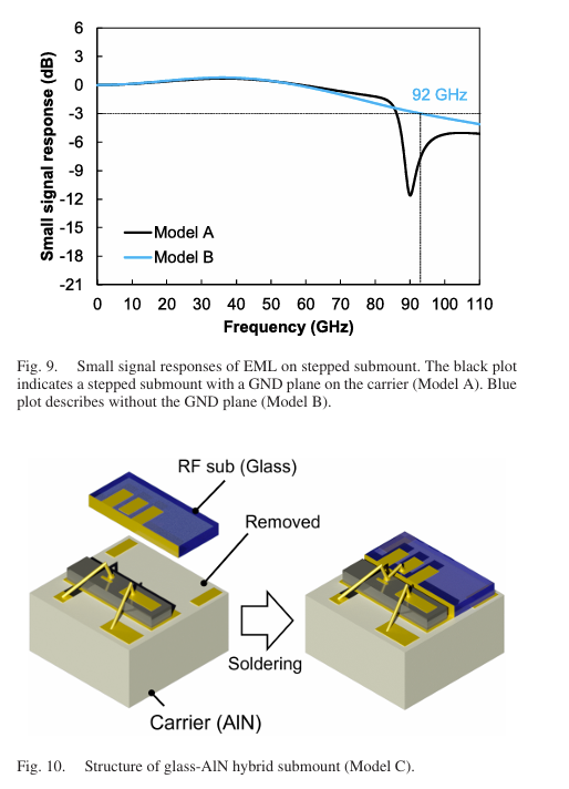

Fig. 13 & Fig. 14 (thermal and optical performance): At 50°C, the P-I curve (Fig. 13) shows no saturation or kinks, and the spectrum (Fig. 14) shows a side-mode suppression ratio (SMSR) above 50 dB. This confirms that the AlN base handles the thermal load well, ensuring long-term device reliability.
Fig. 15 (measured small-signal response of the hybrid substrate): Now for the exciting measured results. With a 1.1 µm-wide EAM (capacitance about 60 fF), measured bandwidth reached 100 GHz, closely matching simulation. With the ultimate 0.8 µm-wide EAM (capacitance down to about 42 fF), 3 dB bandwidth broke right through the 110 GHz limit of the measurement equipment. This establishes the feasibility of 400G/lane with a wire-bonded architecture.

Stage 3: Wire-Bond-Free Packaging for CPO/NPO (Fig. 16 - Fig. 19)
As optoelectronic integration moves toward high edge density, the area taken up by conventional wire bonds has become a luxury.
Fig. 16 (high-density packaging concept): Shows wire-bond-free 3D (junction-up) and 2.5D (junction-down) EML packaging architectures that let the electronic IC (EIC) and photonic IC (PIC) sit much closer together.

Fig. 17 & Fig. 18 (prototype and top view): The team built a junction-up prototype (Fig. 17). So that the RF glass substrate could be bonded directly, they placed ground blocks (GND blocks) of equal thickness on both sides of the EML and used double-stacked Au stud bumps to compensate for a height tolerance of about 10 µm. The top view in Fig. 18 shows a highly integrated design with the termination resistor and peaking inductor monolithically integrated on the glass substrate, with a pitch that supports array expansion at 500 µm.
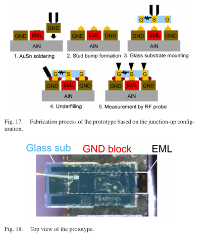
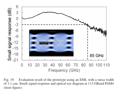
Fig. 19 (measured performance of wire-bond-free packaging): Measured 3 dB bandwidth reached 85 GHz. Because the signal must pass through metal vias in the quartz substrate, and the double-stacked Au stud bumps add extra parasitic inductance, bandwidth is somewhat below the 100 GHz of Fig. 15, but the architecture still produced a clean 113.4 GBaud PAM4 eye (at 1.0 Vpp modulation, estimated TDECQ of 1.8 dB and extinction ratio of 4.9 dB). The authors also note pragmatically that enlarging the via diameter should further reduce parasitic inductance and raise bandwidth.
Conclusion: The Industry's Next Step
Mitsubishi Electric's paper not only shows deep expertise in InP epitaxy and chip design but also lands a well-aimed blow on high-frequency packaging, an often-underestimated link. The Glass-AlN hybrid substrate has very high commercialization potential, letting today's 3.2T pluggable optical modules reach 100 GHz bandwidth while preserving thermal performance and reliability. Its exploration of wire-bond-free CPO packaging also paves the way for ultra-high-density co-packaged optics inside future AI clusters. From the optical communications supply chain's perspective, this means high-power EMLs remain a heavyweight player not to be ignored in the 400G/lane era.


Comments