


VLSI 2026 | Paper Analysis | NVIDIA Uses a "Self-Timed DFE" to Push Optical Receiver Sensitivity to -18.5 dBm at 0.416 pJ/b
At VLSI 2026 (paper C20.4), NVIDIA presented a 32 Gb/s optical NRZ receiver that 3D-stacks a 7nm CMOS electronic IC (EIC) and a 65nm silicon photonics IC (PIC) using hybrid bonding. With a new technique called self-timed decision feedback equalization (STDFE), it reaches -18.5 dBm OMA sensitivity at BER<10⁻¹² with PRBS31, at an energy efficiency of just 0.416 pJ/b and an area of 3360 μm². The point isn't speed — it's sensitivity: every 1 dB of sensitivity saved at the receiver translates directly into laser power saved at the system level. The most elegant part is that it costs almost nothing: the entire STDFE loop adds less than 1 mA.
1. Background: the "receiver piece" of NVIDIA's optical I/O push
When people talk about co-packaged optics (CPO), attention mostly goes to the "emit and transmit" parts — laser sources, waveguides, micro-ring modulators — while the receiver is treated as a supporting player. Yet in an optical link's power budget, laser power is usually the largest item, and what determines how bright the laser must be is precisely how small a signal the receiver can hear. All authors of this paper are from NVIDIA (teams in Santa Clara, Durham and Ridgefield); it was presented at the 2026 IEEE Symposium on VLSI Technology and Circuits as paper C20.4. C20.2 in the same session took the differential transimpedance amplifier (differential TIA) route; C20.4 deliberately chose the seemingly contrarian but actually clever path of a "low-bandwidth front end plus equalization."
2. The core problem: sensitivity is the lever on laser power
The paper's motivation in one sentence: receiver OMA sensitivity = the lever on system laser power. OMA (optical modulation amplitude) sensitivity is the minimum optical signal swing required at the receiver input for a target BER. Given the link loss and extinction ratio (ER) from the external laser source (ELS) to the receiver, the better the receiver sensitivity, the lower the required laser power. Improving sensitivity is therefore not "a circuit team's internal matter" — it directly cuts the most expensive power item at the system level. The paper distills receiver design goals into four points: small input parasitic capacitance CIN, large transimpedance resistance R1, large sampler input swing, and matched delay between data and clock paths.
3. From pain point to concept: how "delay matching" unexpectedly produced a free equalizer
Figure 1 shows the causal chain of "how sensitivity determines laser power" and the receiver's various noise sources. The top half draws the link model: the external laser reaches the receiver through link loss; the minimum usable optical power min(PIN) plus link loss gives the minimum laser power min(PTX), which divided by wall-plug efficiency (WPE) yields the electrical power actually paid. The key insight: design goals can be condensed into "smaller CIN, larger R1, larger data swing vd." This figure translates circuit metrics into the system laser bill and is the starting point for understanding why the paper is worth doing.

Figure 2 shows how limiting amplification suppresses noise at the center of the eye, along with the baseline TIA circuit for comparison. The top shows eye diagrams at nodes v3 and vfe under transient noise simulation: v3 swings less than 100 mV with noise σ of about 6 mVrms, while vfe, amplified to rail-to-rail, swings more than 800 mV with noise σ at the eye center below 3 mVrms. This "rail-to-rail output suppresses center noise" effect is essentially equivalent to the "noise-free decision" concept in a DFE. It reveals an overlooked free resource: the data must be amplified to rail-to-rail anyway for delay matching, and that rail-to-rail signal happens to be a clean decision source for a DFE.

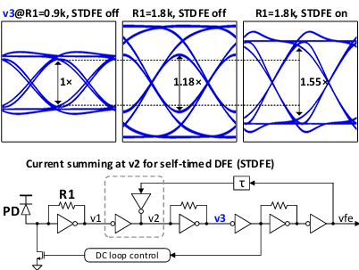
Figure 3 shows the core STDFE concept and how it opens the eye. The top compares v3 eye diagrams in three cases: baseline (R1=0.9k, STDFE off) as the 1× reference; increasing R1 to 1.8k with STDFE still off raises eye opening to 1.18× (low-frequency gain rises but bandwidth drops, adding ISI); with R1=1.8k and STDFE on, eye opening jumps to 1.55×, more than 1.5 times the baseline. The approach drives an inverter with the rail-to-rail TIA output, forming current summation at node v2, which combines naturally with the inverter-based Cherry-Hooper amplifier on the main path. Because the DFE timing is "derived from the data itself," it is called a self-timed DFE.
4. Circuit implementation: TIA and clock-forwarding architecture
Figure 4 shows the TIA circuit as actually implemented, including the high-R1 low-bandwidth front end and STDFE. Conceptually STDFE needs only one inverter from vfe to v2; but to optimize the STDFE loop independently without touching the main signal path, the designers instead tap the signal from node v4, amplify it, and drive a current-injection inverter at v2. The STDFE loop delay is close to 1 UI, and a process- and temperature-adaptive supply is used to reduce delay variation. The circuit uses R1=1.8k, plus a DC loop built from an ultra-low-gm OTA and a 5.3 pF thick-oxide MOS capacitor to achieve a very low high-pass cutoff frequency — which removes the overhead of DC-balanced encoding.

Figure 5 shows the simplified receiver circuit and clock-forwarding architecture. A half-rate clock is received by a clock receiver, which then drives clock distribution across multiple lanes. The same receiver circuit can be configured as either a data receiver or a clock receiver: the rail-to-rail TIA output enters a delay-matching block (DLY), with one branch for data and one for clock; in data mode the data path is enabled, and a feedback inverter is added to improve signal quality into the deserializer (DES). Clock distribution uses an injection-locked oscillator (ILO). This architecture is designed for many lanes in parallel.

5. Measurement results: sensitivity, BER and timing margin

Figure 6 shows the measurement setup: two external Mach-Zehnder modulators (MZMs) modulate lasers with a clock and a PRBS pattern respectively, at extinction ratios of 9.4 dB and 12.7 dB; a 50:50 splitter allows the optical eye to be observed before the PIC. The clock signal enters the PD directly via waveguide, while the data signal passes through a micro-ring resonator (MRR) before reaching the PD; the laser wavelengths measured were 1308.23 nm and 1300.00 nm. The inclusion of the MRR echoes NVIDIA's positioning on DWDM optical paths.

Figure 7 shows the sensitivity improvement of STDFE over the baseline with a PRBS7 pattern. At BER<10⁻¹², STDFE achieves a 2 dB sensitivity improvement over the baseline receiver, at the cost of less than 1 mA of current overhead (clock receiver input OMA of -18 dBm). This is the most persuasive figure in the paper: 2 dB of sensitivity for under 1 mA — at the system level, those 2 dB translate almost directly into laser power that can be cut.

Figure 8 shows BER curves under different PRBS patterns and gives the receiver's final sensitivity figures. At BER<10⁻¹², PRBS31 reaches -18.5 dBm OMA sensitivity and PRBS7 reaches -18.7 dBm. PRBS31 is the more demanding long pattern, and sensitivity drops only 0.2 dB, showing the equalization remains robust under long-range data correlation. A PRBS31-level figure is the threshold real link specs require — meeting it is what qualifies a design for product.

Figure 9 shows the bathtub curve with 1 dB of link margin, quantifying the timing eye opening. With 1 dB of link margin reserved (data receiver input -17.5 dBm OMA, clock receiver input -18 dBm OMA) and a PRBS31 pattern, the bathtub BER curve shows 27% UI of horizontal eye opening at BER<10⁻¹². This means that even with an extra 1 dB of system margin, nearly 30% of the UI remains as timing window, rather than all margin being used up.
6. 3D stacking and peer comparison: Figure 10 and Table I

Figure 10 shows die photos of the EIC and the receiver, and a cross-section of the EIC/PIC 3D stack. The EIC is 7nm FinFET and the PIC is 65nm SOI; the key benefit of hybrid bonding is minimizing parasitic capacitance at the receiver input — exactly the "smaller CIN" from Figure 1. The receiver occupies 3360 μm² and draws 13.2 mA from a 1.01 V supply at 32 Gb/s (regulated down to 0.84 V). 3D stacking is the physical prerequisite for shrinking CIN, which allows a larger R1, which in turn improves sensitivity.
As for the paper's Table I, it places this receiver among its peers: compared with JSSC'18 (-12.4 dBm, 1.41 pJ/b), ISSCC'23 (-11.4 dBm, 0.96 pJ/b) and SSCL'24 (-17.0 dBm, 0.0848 pJ/b), this work has the best sensitivity of the four at -18.5 dBm, and is the only one achieved under the most demanding PRBS31 pattern; its energy efficiency of 0.416 pJ/b (including TIA, DLY and DES) sits in the middle, with CIN of 45 fF, responsivity of 1.0 A/W, and no inductors. The industry signal is clear: NVIDIA chose to bet on "sensitivity" rather than on "the energy-efficiency number alone," because sensitivity is the variable that actually brings the system laser bill down.

Conclusion
The value of this paper isn't whether it is the world's fastest receiver or has the prettiest efficiency number; it's that it demonstrates a "free-found equalizer" design philosophy: since the signal must be amplified to rail-to-rail anyway for clock/data delay matching, reuse that rail-to-rail output as a noise-free DFE decision and build the equalization with a few inverters and current summation, for a total cost under 1 mA. The result is -18.5 dBm PRBS31 sensitivity, 0.416 pJ/b efficiency and a 3360 μm² footprint, all built on hybrid-bonded 3D stacking of a 7nm EIC and a 65nm PIC. STDFE turns "sensitivity" from an internal circuit-team metric into the single most worthwhile investment on the whole optical link's balance sheet.
References
Paper title: A 0.416-pJ/b, 32-Gb/s 3D-Stacked Optical NRZ Receiver with -18.5-dBm OMA Sensitivity Using Self-Timed Decision Feedback Equalization. Authors: Li Xu, Sanquan Song, Nikola Nedovic, Georgios Kalogerakis, Nandish Mehta, Angad Rekhi, Brian Zimmer, Stephen G. Tell, Yoshinori Nishi, Xi Chen, Ward Lopes, Benjamin G. Lee, Thomas H. Greer III, John W. Poulton, C. Thomas Gray (NVIDIA). Conference: 2026 IEEE Symposium on VLSI Technology and Circuits, paper C20.4, 2026 (DOI: 10.1109/VLSITECHNOLOGYANDCIR65830.2026.11577496).


Comments