


Technical Paper Analysis | Silicon Microring Modulators Enter the 200Gb/s Era: NVIDIA's Design Philosophy and Trade-offs
1. Introduction: Why Microring Modulators Are CPO's Chosen One
As AI factories scale, traditional pluggable optical modules are showing their limits in power and density. CPO (co-packaged optics) is seen as the ultimate answer, offering up to 5x better power efficiency and 10x better resiliency. Among modulator options, MRMs stand out for their tiny footprint and high bandwidth density, and they are highly compatible with CMOS processes - making them especially well suited to 3D integration through processes such as TSMC's COUPE (Compact Universal Photonic Engine).
But to break 200 Gb/s per lane, designers must perform an extremely complex co-optimization across electrical bandwidth, optical loss, linearity and modulation efficiency.
2. Source
Title: Si Microring Resonator Modulators at >200Gb/s
Author: David Patel
Affiliation: NVIDIA
Venue: OFC 2026 (Optical Fiber Communication Conference)
3. In-Depth Figure Analysis
Figure 1: Electrical Model and the Physical Limits of 3D Integration
This figure reveals the underlying logic of MRM electrical performance:

Figures 1a & 1b (circuit model and transfer function):
Modulation bandwidth is mainly limited by the PN junction resistance and capacitance.
Ignoring parasitics, the response approximates a single-pole RC model. To break through the bandwidth limit, the industry has started adopting electrical inductive peaking.
Figure 1c (efficiency vs. capacitance trade-off):
This is a "bitter" compromise: increasing doping concentration lowers R_j (raising bandwidth), but increases optical loss, and the junction capacitance C_j shifts as well.
Figure 1d (3D IC structure):
Shows EIC (electronic IC) and PIC (photonic IC) stacking achieved through TSMC COUPE/SoIC hybrid bonding.
Why it matters: this 3D integration drastically shortens the electrical signal path and reduces RLC parasitics, which is critical for ultra-high-frequency signals above 200 Gb/s.
Figure 2: Optical Dynamics and EO Peaking

The optical response of MRMs is not linear and is strongly affected by thermal effects:
Figure 2a (pole-zero analysis):
The small-signal response is determined by a pair of complex-conjugate poles and one zero.
Figure 2b (effect of coupling regime):
Shows the response differences between undercoupled and overcoupled rings at different biases.
At high power, due to optical self-heating, the modulator can usually only operate on the short-wavelength side of the resonance.
Figure 2c (EO peaking and detuning):
Key insight: reducing detuning (moving the laser closer to resonance) increases extinction ratio (ER) but lowers bandwidth.
EO peaking occurs when the modulation sidebands align with the cavity resonance, so DC OMA (optical modulation amplitude) and bandwidth cannot both be optimized at once - designers must seek the optimal gain-bandwidth product.
Table 1 & Figure 3: A Showdown of PN Junction Designs
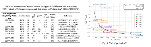
This is the most valuable data comparison in the paper:
Junction structures compared: covers LPN (lateral), VPN (vertical), ZPN (Z-shaped), mPN (meandered) and CAP (SISCAP/MOSCAP) designs.
Performance data:
One of the current record holders reaches 290 Gb/s (LPN), with a V_pi L of 0.9 V-cm and a capacitance of only 10 fF.
Distribution in Figure 3: most junction designs fall on the same trade-off curve. Designs in the lower-left corner (low V_pi L and low C_j) represent today's best technology direction.
Conclusion: chasing phase-shift efficiency (low V_pi L) at the cost of higher loss is offset by reduced cavity enhancement, so holistic co-optimization is what wins.
4. Conclusion: The Road Beyond 1.6 Tbps
NVIDIA's paper makes one thing clear: the future of microring modulators is no longer a solo act.
3D integration is table stakes: reducing parasitics through processes such as TSMC COUPE is the physical prerequisite for >200 Gb/s.
Electronic-photonic co-design: using inductive peaking and non-linear equalization to compensate for nonlinearities caused by optical dynamics.
Accurate modeling: as the physics grows more complex (e.g., TPA and FCA effects), accurate integrated electro-optic-thermal models supporting Verilog-A will become a standard designer tool.
Microring modulators have officially crossed the single-lane 200G threshold, paving the way for next-generation 1.6T and even 3.2T CPO switches.


Comments