


Paper Analysis | Silicon Photonics Transceiver Design Finally Runs at 64 Gbps in a Standard Circuit Simulator
Photonics and electronics have long been two design worlds that barely talk to each other. Photonics engineers model waveguides and modulators in Lumerical and Interconnect; electronics engineers run circuits in Cadence and ADS. In between, data is shuttled by hand, S-parameters are matched manually, and results are copy-pasted back and forth. Meanwhile silicon photonics masks are expensive and tape-out cycles are long, so a single design mistake can cost months and millions. That is why electro-optic co-simulation (EO co-sim) has always been the most critical, and hardest to fill, missing piece in silicon photonics transceiver design.
In this 2025 IEEE Journal of Microwaves paper, Kawahara and Baba of Yokohama National University fill exactly that gap. They built a complete, experimentally validated, and fully open-source Verilog-A photonic component model library that lets silicon photonics transceivers run directly in standard electronic circuit simulators (ADS, Cadence, Synopsys, Keysight), pushing the signal rate to 64 Gbps, beyond the 50 Gbaud threshold that defines the 800G/1.6T generation.
The real value of this paper is not "yet another Verilog-A model." It is that it builds in, and validates against real hardware, the two things everyone before had skipped: RF high-frequency behavior and noise.
1. Why This Paper Matters Now
Terabit Ethernet demands symbol rates above 50 Gbaud plus compact packaging, so electro-optic integration is no longer optional. Yet today's electronic and photonic simulators are fragmented: two toolchains, two sets of models, with manual data exchange in between, which is slow and error-prone.
The industry knows the answer is co-simulation in a single environment: write photonic components as Verilog-A models and run them inside electronic EDA. The problem is that earlier attempts had two fatal flaws:
First, early work only established the theory of simulating light propagation in circuit simulators with equivalent baseband models, but did not reflect real device characteristics. Optical loss, back-reflection, nonlinearity, high-frequency response and noise, all indispensable for real design, were missing.
Second, although later work modeled passive components, modulators and photodetectors individually, those models were built in isolation and never unified into a single library, and most details were never published. The authors call it out directly: the most advanced photonic model library today is GlobalFoundries' Fotonix, yet its Si MZM optical link simulation only reaches 26.5 Gbaud, has no noise modeling, and discloses few details, which makes it inadequate for next-generation 800G/1.6T systems.
That is this paper's entry point: a co-simulation library that is unified, experimentally validated, and fully open in both details and source code.

This figure shows the library's design philosophy: models are written in Verilog-A and are therefore interoperable across tools. On the left they connect to silicon photonics fab components, on the right to an electronics foundry PDK, with the photonic model library acting as the bridge. It is not a closed solution locked to one foundry but an open, composable layer.
2. The Core Problem This Paper Solves
In one sentence: make photonic components simulate as accurately as transistors inside standard electronic circuit simulators, accurately enough to design real transceivers above 50 Gbaud.
The biggest technical obstacle is frequency scale. The optical carrier ωO is as high as 193 THz (λ = 1550 nm) while electrical signals are only tens of GHz. That gap of four orders of magnitude would require astronomical sampling rates if simulated directly. The fix is an equivalent baseband model: shift the optical carrier by a reference frequency ωref and keep only the slowly varying envelope relative to ωref, bringing the number of transient time steps down to a manageable level. Complex values and bidirectional propagation are represented with a 4-bit bus E[0:3] (forward real, forward imaginary, backward real, backward imaginary).
The baseband framework itself is not new. The real engineering work comes next: putting every component's real physical behavior into that framework and then matching it to measurements.
3. Key Figures, One by One
Rib MZM: Modeling Traveling-Wave Electrode Loss Segment by Segment

This figure shows why MZMs are so hard to model: you need the RC time constant, RF loss, optical and electrical group delay, and electrode characteristic impedance all at once. That is why most earlier Verilog-A MZM models stalled at 25 Gbaud. The authors split the 2.0 mm traveling-wave electrode into 40 cascaded 50 μm segments, using a distributed model that simultaneously captures RF propagation loss, impedance mismatch, and the phase mismatch between the optical and RF signals.
The key is in the subcircuit details. They model both the metal line's skin effect and the substrate's eddy current loss: L1/R1 are the line inductance and resistance, L2/R2 capture the parasitic resistance rise from skin effect at high frequency, C1 is the substrate capacitance, and C2/R3 model the drop in high-frequency shunt impedance caused by eddy currents. These parameters are extracted with Keysight Momentum EM analysis; the p-n junction Rpn and Cpn are extracted with Ansys Lumerical charge-transport simulation, and the bias dependence of Cpn (depletion-region expansion) is modeled with a polynomial.

This figure shows the result of the parameter extraction: by handling skin effect and eddy current loss correctly, the RF propagation constant γRF fits well up to 40 GHz, and the voltage dependence of Cpn is captured correctly, which is a prerequisite for accurate frequency-response simulation. For silicon photonics engineers the message is concrete: MZM high-frequency accuracy is not magic; it comes from faithfully modeling skin effect, eddy currents, RC, and Cpn nonlinearity.
PCW MZM: A Neat Trick for Putting Slow-Light Enhancement into a Circuit Model

This figure shows the Baba group's signature technology: photonic crystal slow light. Slow light strengthens light-matter interaction, and the phase shift Δφ is proportional to the group index ng. The authors use an elegant approximation in the model, replacing the first-order voltage coefficient of the refractive index n1 with (ng/ng_ref)·n1 to emulate slow-light enhancement. The rationale is straightforward: slow-light bandwidth ranges from a few nm to tens of nm with ng dispersion of 10-100, while the RF signal bandwidth is only about 50 GHz (roughly 0.4 nm at a 1550 nm center), far smaller than the slow-light dispersion scale. Group velocity dispersion within the signal band is therefore negligible and a first-order approximation suffices.
To improve phase matching between slow light and the RF signal, the phase shifter is split into two sections with an RF delay line in between. The sections are electrically isolated by undoped passive PCW, with a waveguide model added to compute the optical delay, and the transitions are modeled by inserting an optical reflector with 7.5% reflectivity.
Experimental Validation: Standalone Matches to 40 GHz; Co-Packaged, Even the VNA Artifacts Disappear

This figure shows the model's accuracy. For the standalone rib modulator, simulation (solid lines) and measurement (dots) broadly agree from DC to 40 GHz, including the voltage dependence across biases. There is about a 1 dB gap below 20 GHz and a measurement-only spike at 38 GHz, which the authors candidly attribute to calibration error from reconnecting port 2 and bending the RF cable during measurement, not to the model.
The co-packaged case is even more convincing. They designed a driver in 130 nm BiCMOS (IHP foundry), co-packaged it with the PCW modulator, and designed the whole assembly through co-simulation. Measured and co-simulated EO gain agree all the way to 40 GHz, and the discrepancy seen in the VNA case disappears entirely. In effect, this library can be used to design real co-packaged transceivers, not just demos.
Eye Diagrams: Adding Physical Effects One at a Time, Watching the Eye Open and Then Blur with Noise

This is the most instructive figure in the paper. Starting from a clean PRBS eye, it adds optical group delay, RC time constant, traveling-wave electrode, jitter and driver, ASE noise, and thermal noise step by step. You can clearly see optical group delay and the RC time constant squeeze the eye shut, the traveling-wave electrode, by matching the optical and RF signals, open it back up, and finally jitter and noise blur the waveform into something close to the real measurement. The final extinction ratio (ER) error is under 1 dB.
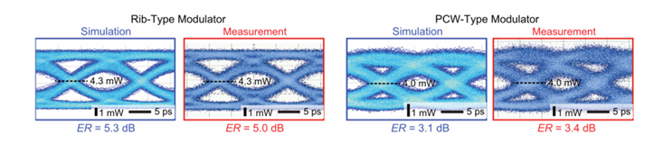
This figure wraps the story at 64 Gbaud: simulation and measurement agree under all conditions with ER error <1 dB, proving the model can accurately predict link performance above 50 Gbaud, aimed squarely at 800G, 1.6T and beyond.
4. Technical Highlight: Filling In Noise, the Long-Ignored Missing Piece
If you had to pick this paper's most underrated yet most critical contribution, it would be building test-equipment noise into the co-simulation. Previous Verilog-A optical link simulations almost always skipped this, even though it has a huge impact on BER.
EDFA ASE noise is modeled as PASE = μhνΔν(GEDFA−1), with the coefficient μhνΔν determined by least-squares fitting to measurements as 3.44×10⁻¹⁹ W/Hz, and the noise generated with a Gaussian random function. The tunable filter is a sixth-order Butterworth with 2 nm bandwidth, using a clever "shifted reference frequency + complex multiplier" technique to work around Verilog-A's lack of complex-number support. The photodetector module is even more interesting: the measured RMS noise voltage is Vrms = 65 μV and independent of received optical power, which directly shows that the dominant noise sources are the TIA and ADC, not photodiode shot noise.
Only with this real noise built in do the eye diagrams blur the way real hardware does, and only then are BER predictions meaningful. This is the most fundamental difference between this library and earlier simulations that were unrealistically clean.
5. Industry Implications: What This Means for Fabless Silicon Photonics Designers
Zooming out to the supply chain, the paper matters on three levels.
First, it lowers the barrier to EO co-design. Designing a silicon photonics transceiver used to require expensive photonic EDA licenses and a cross-disciplinary electro-optic design team. An open-source model library that runs in standard electronic EDA (ADS/Cadence/Synopsys) now lets more fabless design houses validate links to 64 Gbps before tape-out, saving not just money but several tape-out cycles.
Second, it punctures the comfort zone of closed PDKs. The authors use GlobalFoundries Fotonix as the benchmark: the most advanced, yet limited to 26.5 Gbaud, without noise modeling, and with undisclosed details. An open, verifiable library reaching 64 Gbps is a direct counterexample to the assumption that photonic PDKs must be foundry-locked and closed-source.
Third, it demonstrates a complete design loop for co-packaged transceivers. From the PCW modulator to the co-packaged 130 nm BiCMOS driver, the whole assembly was designed via co-simulation and matched to measurements up to 40 GHz. That "simulate first, then tape out" capability is exactly what CPO and co-packaged optics need as they move toward volume production.
6. Verdict
The paper's place in the technology timeline is clear: it is the first silicon photonics EO co-simulation library that fully models RF high-frequency behavior and noise, is validated against hardware up to 64 Gbps, and is completely open source.
It is not a new modulator, nor a record-breaking bandwidth number. Its weight lies in moving silicon photonics transceiver design from a fragmented state, with photonics and electronics in separate silos and data moved by hand, a big step toward accurate co-design inside a single standard electronic EDA environment. For an optical communications supply chain racing toward 800G/1.6T while struggling with tape-out costs and electro-optic integration complexity, the ability to move validation ahead of tape-out hits closer to the real pain point than any single technical breakthrough.
Slow light, open source, noise modeling: with these three keywords together, this paper deserves a place in your silicon photonics design toolkit.
References
K. Kawahara and T. Baba, "Electro-Optic Co-Simulation in High-Speed Silicon Photonics Transceiver Design Using Standard Electronic Circuit Simulator," IEEE Journal of Microwaves, vol. 5, no. 4, pp. 983–995, Jul. 2025. DOI: 10.1109/JMW.2025.3576358. The model library and example testbenches (Keysight ADS) are open source on GitHub: github.com/keikawa/Verilog-A-photonic-model-library
(Publish after images are added: insert the corresponding figure files in the Wix dashboard at each [Paste Fig. X] placeholder in the text and credit the source.)



Comments