


ECTC 2026 | Tohoku University | Chemically Tailored Cu-Electroplating and Contactless Isostatic Annealing of 1-mm-Thick Full Glass Wafer Cu Through-Glass-Vias
To use glass substrates as advanced packaging interposers, one hard problem has to be solved first: how to fill deep, straight through-glass vias (TGVs) with copper, leave no voids, and make the copper good enough. Japan's Tohoku University presented a complete solution at ECTC 2026. Step one uses electroless nickel plating as the sidewall seed layer (replacing unevenly covering sputtering), achieving uniform coverage even in straight vias with aspect ratios up to 100:1 in 1 mm-thick glass. Step two uses chemically tailored modified conformal electroplating (MCEP) — a purpose-formulated Bath B suppresses current crowding at the via mouth, prevents premature pinch-off and fills the via with copper top to bottom without voids. Step three is the cleverest: hot isostatic pressing (HIP) annealing replaces conventional furnace annealing, growing very large copper grains (>40–45 µm) with a low Young's modulus (<60 GPa) — large grains conduct better and soft copper absorbs thermal stress, a win for both reliability and electrical performance. In one sentence: Tohoku University clears both glass TGV hurdles — “fully filled” and “good enough copper” — in one go with electroless nickel, chemical electroplating and HIP annealing.
1. Background: The First Hurdle for Glass Interposers Is TGV Copper Fill
This paper comes from Tohoku University (Sendai) with T-Micro and JCU, presented at the 2026 IEEE 76th ECTC. The glass interposer process flow resembles that of silicon interposers in three major blocks: etching the vias (TGVs), copper fill + CMP, and building the RDL. TGVs come in straight and butterfly shapes; high-density interconnect arrays require straight vias, but straight vias are deep and hard to fill.
Two long-standing problems: first, the seed layer — sputtering (PVD) covers high-aspect-ratio straight vias poorly, so sidewall Ti/Cu often breaks and the middle section goes unplated; second, via filling — conventional baths plate too fast at the via mouth, pinching it off early and leaving voids in the middle. For the race to use glass as an advanced packaging substrate, see Glass Substrates Are No Longer Slideware: Why the TGV Race Comes Together in 2026; for the full picture of packaging-side integration, see CPO Is Won in Packaging, Not Optics — John Lau on PIC/EIC Heterogeneous Integration.

2. The Core Question: The Whole Paper in One Sentence
What this paper sets out to prove: can high-aspect-ratio straight TGVs in 1 mm-thick glass be filled with copper void-free, with large grains, good electrical performance and good reliability?
The answer is yes — through three moves: an electroless nickel seed layer + chemically tailored electroplating (MCEP) + HIP annealing.
3. Key Figures, One by One
3.1 This Figure Shows That “an Electroless Nickel Seed Layer Solves Sidewall Coverage”

This set of figures (Fig. 2) covers the seed layer. The hardest part of high-aspect-ratio straight TGVs is depositing a uniform adhesion/seed layer; without it you can't make liquid-tight or helium-tight vias. The team optimized the bath temperature, pH and concentration of electroless nickel (EL-Ni) to deposit a continuous, conformal nickel film on the sidewall SiO₂ — 1.7–2 µm of nickel inside A/R 10, 100 µm-diameter vias, with conformality of 0.85. That 85% sidewall coverage is enough for the subsequent copper electroplating to fill completely. Electroless nickel is cheaper and more reliable than sputtering, and it is the key to getting around PVD's coverage limits.
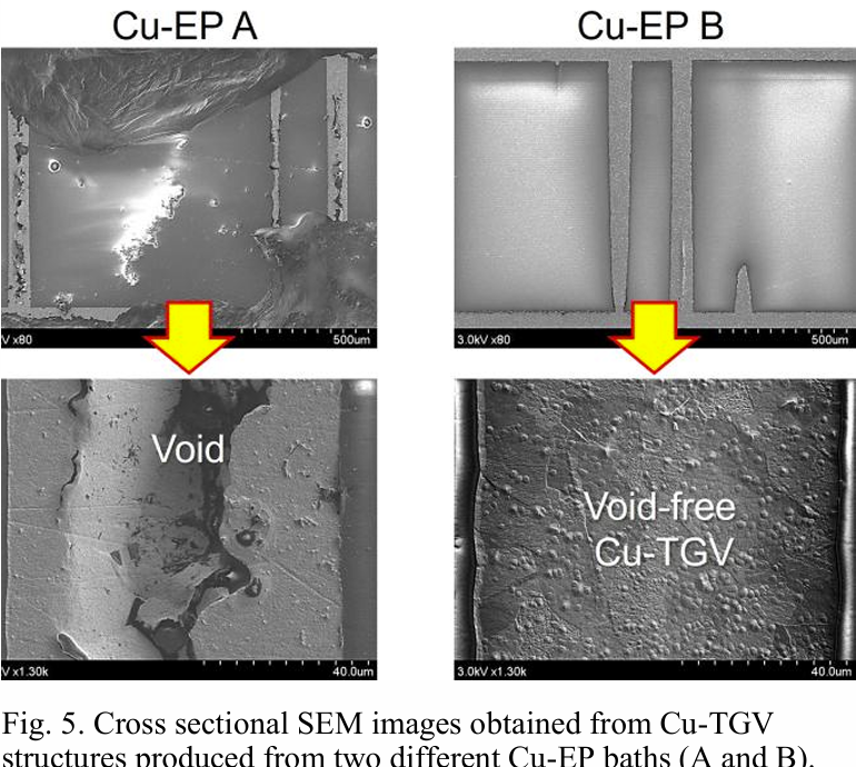
3.2 This Figure Shows That “Chemically Tailored Electroplating Fills the Via Void-Free”
This set of figures (Fig. 4, Fig. 5, Fig. 10) covers via filling, comparing two baths: Bath A (optimized for bottom-up blind-via filling) has high copper ion concentration and plates too fast at the via mouth, causing severe mid-via pinch-off and many voids; Bath B (MCEP) has low copper ion concentration, suppresses current crowding at the mouth, anchors leveler molecules uniformly on the sidewall, and deposits copper evenly from top to bottom — void-free and nearly seamless. Resistance: about 5 mΩ for Bath A (with voids) versus about 3.5 mΩ for Bath B — even lower than the calculated value, showing that Bath B achieves near-superconformal filling.
Key point: via filling isn't about plating more; it's about using chemistry to keep the via mouth from plating too fast.


3.3 This Figure Shows That “HIP Annealing Grows Very Large Copper Grains and Softens the Copper”


This set of figures (Fig. 9, Fig. 10, Fig. 12) covers annealing. Conventional atmospheric furnace annealing yields small (<15 µm), disordered copper grains containing non-metallic phases. After switching to hot isostatic pressing (HIP, 20 MPa N₂) annealing, Bath B copper grains are very large (>45 µm) with strong crystallographic orientation — critical for low-resistance TGVs. And post-HIP copper has a low Young's modulus (<60 GPa) and is softer, absorbing thermal stress during thermal cycling and improving the thermomechanical reliability of the glass substrate. Large grains conduct better, soft copper resists thermal stress — a win for both electrical performance and reliability.
4. Technical Highlights
The first highlight is an electroless nickel seed + MCEP chemical via filling: cheap, reliable electroless nickel solves sidewall coverage in high-A/R straight vias, and the purpose-formulated Bath B suppresses current crowding at the mouth to fill void-free — filling hard-to-fill straight TGVs nearly seamlessly in a single step.
The second highlight is grain engineering via HIP annealing: contactless hot isostatic annealing grows >45 µm grains with a low Young's modulus, delivering both low resistance and good thermomechanical reliability. This extends “fully filled” to “good enough copper,” the key to making glass TGVs truly usable.
5. Industry Link: How Far from Volume Production? Who Benefits?
Distance: maturity sits at the “materials/process validation” stage — filling, resistance, grain size and Young's modulus have all been verified, using electroless and electroplating chemistries and HIP annealing that lean toward manufacturability. But this is a process demonstration by academia and equipment partners; yield across full 1 mm-thick glass wafers, RDL integration and the link to real interposer products still lie ahead.
Beneficiaries: most directly the glass substrate/TGV and electroplating chemistry ecosystem (echoing Corning and the materials side of the TGV race), plus packaging houses looking to use thick glass for high-frequency/high-performance interposers or display applications. A note of caution: glass TGVs compete and coexist with silicon TSVs and organic interposers as different routes — glass wins on low loss, low dielectric constant, thick substrates and large panels, but brittleness, integration with existing CMOS/packaging lines and volume yield are still to be proven. This paper addresses the foundational bottleneck of “glass TGV copper fill.”
6. Conclusion
The one line to remember from this paper: Tohoku University clears both glass TGV hurdles — “fully filled × good enough copper” — in one go with an electroless nickel seed + chemically tailored electroplating (MCEP) + HIP annealing: even straight vias at A/R 100:1 in 1 mm-thick glass fill void-free and grow >45 µm grains. For anyone tracking glass substrates, the watch point is this: before glass can take over, the foundational TGV copper-fill process has to be stable with good copper grains, and Tohoku University has pushed that a big step forward.
References
Murugesan Mariappan, Hiroyuki Hashimoto, Takafumi Fukushima et al. (Tohoku University), with Kiyoharu Mori (T-Micro) and Masahiro Sawa, Jinta Nampo (JCU), "Chemically Tailored Cu-Electroplating and Contactless Isostatic Annealing of 1-mm-Thick Full Glass Wafer Cu Through-Glass-Vias," 2026 IEEE 76th ECTC.
Related Reading
Glass Substrates Are No Longer Slideware: Why the TGV Race Comes Together in 2026: the full picture of glass substrates and TGVs
CPO Is Won in Packaging, Not Optics — John Lau on PIC/EIC Heterogeneous Integration: context on packaging substrates and integration


Comments