


Paper Analysis | CPO Is Won in Packaging, Not Optics: John Lau Maps Every PIC/EIC Heterogeneous Integration Approach
As optics moved from pluggables at the edge of the switch all the way to sitting "face-to-face" with the ASIC, this stopped being the optical engineer's game long ago. It belongs to the packaging engineer now.
This review by John H. Lau (ASME Fellow, Unimicron), published in the Journal of Electronic Packaging (March 2025), has no flashy new data, but it does something very valuable for the industry: it lays out, in one place, every approach to how CPO integrates the photonic IC (PIC) and electronic IC (EIC) with the switch ASIC. From 2D side-by-side, to adding bridges, to 3D stacking and glass substrates, it is effectively a full map of CPO packaging technology.
This guide walks you through that map and answers one core question: why the deciding factor in CPO is shifting entirely from the "optics" side to the "packaging" side.
1. Why this paper is worth reading now
The problem isn't insufficient bandwidth or weak lasers. It's distance.
Pluggable transceivers have carried the industry for nearly 30 years, evolving from the 1995 GBIC to today by plugging optical modules into the edge of the PCB. But as AI data centers pushed switch chips from 25.6T to 51.2T, the architecture's fatal flaw got amplified: the PIC/EIC sits too far from the ASIC, so signals travel a long copper path across the PCB, degrading power, latency and signal integrity.
The entire point of CPO, in one sentence: move the optical/electrical engine as close to the ASIC as physically possible. We broke this down fully in CPO Is No Longer "Crying Wolf": NVIDIA's Volume Production and the Scale-Up Endgame (in Chinese), and Lau's paper is essentially the packaging handbook behind that "endgame."
Lau first pins down the terminology, which is the basis for reading every figure that follows:
Optical engine (OE) = PIC: the optical side, including the PD (photodetector) and laser
Electrical engine (EE) = EIC: the electrical side, including the driver and TIA (transimpedance amplifier)
ASIC: the switch chip itself
What CPO has to solve is how to place and connect these three pieces: OE, EE and ASIC.
2. The evolution in one figure: Pluggable to OBO to NPO to CPO
This is the single most important figure to understand first. It has only one storyline: the PIC/EIC keeps moving closer to the ASIC, and every step closer brings a step up in power and electrical performance.
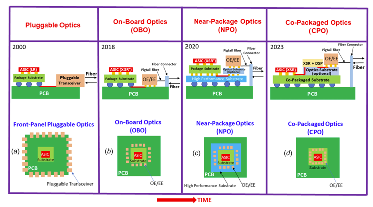
The four stages:
Pluggable (2000 onward): modules plug into the PCB edge, farthest from the ASIC, with the worst power and electrical performance
On-board optics, OBO (2018 onward): the OE/EE move onto the same PCB as the ASIC, arranged around it and connected through the PCB — a step closer
Near-packaged optics, NPO (2020 onward): the OE/EE move next to the ASIC on the same high-performance substrate. Per OIF specs, the ASIC-to-optics distance is at most 150 mm with a 13 dB channel loss limit
Co-packaged optics, CPO (2023 onward): officially launched once Intel and Broadcom shipped. The OE/EE sit tightly along all four sides of the ASIC on the same co-packaged substrate. Per OIF, module-to-ASIC distance is limited to 50 mm with a 10 dB channel loss limit — 3 dB less than NPO
NPO vs. CPO in one line: NPO pulls the optics up next to the ASIC package; CPO puts the optics and the ASIC die side by side inside the same package. CPO wins across the board on form factor, power and latency.
For when CPO went from "crying wolf" to commercial reality, see CPO's First Commercial Year Begins: TSMC COUPE Volume Production and the 200G EML Bottleneck (in Chinese).
3. The real battlefield: three ways to integrate PIC/EIC with the ASIC
Once distance is solved, the next question appears immediately: with the OE/EE and ASIC side by side on one substrate, how do you actually connect them? Lau splits 2D (side-by-side) integration into two main schools.
School 1: Pure side-by-side, differing by substrate class

Placed directly on a standard co-packaged substrate, using μbumps or C4 bumps
Placed on a TSV-interposer or organic-interposer — a TSV-interposer is called 2.5D IC integration; an organic-interposer is called 2.3D IC integration
A package substrate is stacked on top of the interposer before finally connecting to the PCB
One key trade-off worth remembering: 2.5D (TSV-interposer) outperforms 2.3D (organic-interposer), but it also costs more. This cost/performance line is exactly where interposer vendors position themselves — for how POET uses an optical interposer to break in, see our dedicated piece Breaking Down the POET Optical Interposer (in Chinese).
School 2: Adding a bridge
When you don't want to pay for a full, expensive interposer but still need localized high-density interconnect, the bridge comes in. Lau lists three types:
Si bridge + μbump: the most straightforward bridge
Si bridge + Cu-Cu bumpless hybrid bonding: removes the μbumps for another step up in density
Intel EMIB: the bridge is embedded in a substrate cavity, and the chips carry both μbumps and C4 bumps
The spirit of the bridge approach: don't pay for an entire interposer just for a handful of high-density connections.
4. Hitting the wall: why 51.2T has to stack
This is the section with the most industry tension.
The standard CPO layout puts the ASIC on an organic substrate surrounded by 16 OE/EEs. Run the numbers and the problem is obvious:

Today's 25.6T switch: needs 16 OE/EEs @1.6 Tbps
Next-gen 51.2T switch: needs 16 OE/EEs @3.2 Tbps, and each EIC/PIC is larger
Here's the problem: multi-chip module (MCM) size has a physical limit, and with today's packaging technology there's barely room to surround a 51.2T ASIC with 16 OE/EEs @3.2T. If 2D side-by-side can't fit, the only way out is up — stacking the PIC and EIC (3D stacking) to trade vertical space for horizontal area.
Here Lau presents nine 3D stacking configurations (Fig. 14, a through i), differing in stacking direction, the use of μbump / C4 / TSV / hybrid bonding, and whether an extra interposer is added. The point isn't to memorize nine arrangements but to grasp one principle:
Fewer TSVs, fewer bumps, and hybrid bonding wherever possible — because that means higher density, shorter paths and better thermals.

And the most complex CPO in public data so far, Lau notes, is NVIDIA's — SoC, HBM, EIC and PIC all 3D-integrated on a TSV-interposer, with a single OE packing 24 NVLINKs, 4.8 Tbps per direction and 24 laser fibers in a 5 mm x 10 mm footprint.
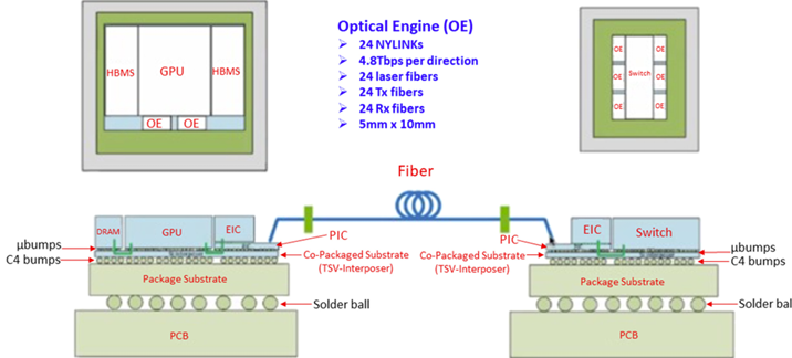
OpenLight's CEO has made the same "3D stacking is the real scale-up window" call from a different angle — breaking out five convergence thresholds and arguing that only vendors capable of 3D stacking will capture the 7–10x volume expansion of scale-up. For the full context, see The 3D Photonic Integration Watershed: OpenLight CEO's Five Convergence Thresholds (in Chinese). Lau from packaging and OpenLight from photonic convergence arrive at the same conclusion by different routes: the 51.2T wall can't be cleared in 2D.
3D versions with bridges (Si bridge, EMIB, and fan-out embedded bridges that bury a Si bridge in a fan-out substrate and connect through TMVs) are also covered, following the same logic as the 2D set, just in three dimensions.
5. The next bet: glass substrates
If 3D stacking is the present tense, glass substrates are Lau's bet on the future tense.
Intel formally announced its glass substrate technology on September 18, 2023, targeting one trillion transistors in a single package by 2030. Why does the optical communications world care so much about glass? Because it offers PICs several advantages organic substrates can't:
Smoother, flatter surface
Optical waveguides can be built directly in the glass, guiding light straight to the PIC's PD and laser devices — this is critical for CPO
Better optical properties and superior thermal, mechanical and dimensional stability
Higher interconnect density, with improved signal speed, power delivery and design rules
But Lau doesn't only report good news. Citing Intel EVP Ann Kelleher, he flags three real hurdles: glass is more expensive than mature organic substrates, early yields will be an issue, and an entire ecosystem must be built from scratch (equipment, materials, supply, even outsourced assembly and test).
In other words, the technical advantages of glass substrates are clear, but they're stuck at the "great technology, but the ecosystem hasn't grown yet" stage — a classic "right technology, wrong time" risk.
6. Conclusion
The whole paper in one sentence: CPO is a packaging problem, not an optics problem.
Lau's own definition of the essential 2D vs. 3D difference is clean — in 2D the PIC/EIC sits side by side with the ASIC on the substrate; in 3D the PIC/EIC is stacked. The four benefits and three costs of 3D are worth writing down:
3D benefits: better performance, smaller package, higher density, fewer bridges needed.
3D costs: harder assembly, tougher thermals, higher assembly yield loss.
This also defines where CPO's real battlefield is. The hard problems Lau calls out — on manufacturing, the biggest challenges are "fiber coupling for ultra-high-density optical I/O" and "light source integration"; on reliability, the "solder joint reliability" of the huge number of interconnects in a CPO structure; on design, balancing "power savings vs. cost savings" and "interoperability standardization." Not one of them is a pure optics problem; all are packaging and integration problems.
This fits exactly with what we discussed in PIC Magazine 2026 Issue 2 Digest: Optical Communications Is Becoming "Semiconductorized" (in Chinese): optical communications is being "semiconductorized," with value and barriers to entry shifting toward advanced packaging. Lau's paper fills in the technical foundation of that trend from a packaging engineer's perspective.
So how should you look at it now? Next time you evaluate a CPO stock, don't just ask how good its optical specs look. Ask three harder questions: Can it do 3D stacking? Is its interposer bet on 2.5D or 2.3D? Has it secured a position in the glass substrate ecosystem? Only the players who can answer those three will get a real slice of the post-51.2T pie.


Comments