


SEMICON Taiwan 2026 Silicon Photonics Global Summit: All 14 Talks Decoded | The Architecture War Is Over, the Manufacturing War Begins
On August 31, 2026, the SEMICON Taiwan Silicon Photonics Global Summit ran a full day in Taipei with 14 technical talks. The most telling signal was not on any slide but in what was missing: not a single talk debated whether CPO should be done.
For the past five years the standard script on this topic went like this: the pluggable camp said CPO is unreliable, the CPO camp said pluggables have hit the wall, and each side got half the stage. Not this time. All 14 talks were built on the same premise (optics is moving into the package, and that is settled) and each went on to explain "how to actually build it."
Even more telling was where the agenda's weight fell: of the 14 talks, 4 (Onto, ficonTEC, Advantest and Enlitech) were devoted entirely to metrology and test. Add the second half of ASE's talk and Lam Research's yield section, and well over a third of the agenda was about "how to mass-produce photonics" rather than "what photonics can do."
Only three things were really decided that day:
The architecture war ended in "coexistence", with Cisco laying out a concrete timeline: CPO starts at the 3.2T generation while pluggables live on
400G/lane is a materials problem, not a design problem, and UMC ruled out all three silicon modulator options one by one
The real bottleneck is not optics but test and yield learning, which happens to be Taiwan's home turf
This is a free full-length STT article. If you want breakdowns at this level every week: check out before 9/30 with code invest2026 and STT PRO annual drops from $1,500 to $1,350, and as long as you renew without a break, you keep that price every year. → See plans on vocus (in Chinese)1. Three Main Threads: What Was Actually Decided That Day
First, why "nobody arguing about architecture" is itself the news.
Summit chair Kuo-Chin Hsu, TSMC Vice President of Advanced Packaging Technology Development, opened with a few numbers: optical transceiver sales grew 25% in 2025 over 2024, and 2026 is expected to surge again by 50%. Looking only at the high-end market above 100G, it doubled in 2024 and grew another 60% in 2025, "driven entirely by AI scale-out." Silicon photonics will take more than half the market by 2027.
The numbers themselves are not news. The news is what he said next: "Industry leaders recently announced that CPO will enter volume production in the second half of this year. The semiconductor world has gone all-in on this path." The summit's very first address treated CPO as a done deal, and none of the following 14 talks circled back to question it.
So the day's content naturally split into three blocks, which is also the structure of this article:
The demand side (Part 1: why optics is unavoidable), the supply side (Part 2: the 400G/lane materials war), and the manufacturing side (Part 3: test and metrology, the real bottleneck).
Thread one: the architecture war ended in coexistence. Cisco spent a full five minutes taking apart four "industry myths," and the verdict on each was "both sides are half right." ASE gave quantified benefit boundaries: 32x the bandwidth at 1/6 the energy. This is not a compromise; the industry has finally accepted the reality that different use cases call for different architectures.
Thread two: 400G/lane is no longer a design problem. UMC Vice President Wen-Chi Ting gave the day's most technically dense talk, ruling out all three silicon modulator paths (MZM, micro-ring (MRM) and SiGe EAM) one by one, each for reasons of physics, not lack of engineering effort. imec, Soitec, Lam Research and Lumentum made the same point from different angles: the next leap in bandwidth will come from materials, not design tricks.
Thread three, and in my view the most underrated signal of the summit: the bottleneck has shifted from "can it be built" to "can it be mass-produced," and the mass-production challenge is test. ficonTEC President Andre Lalonde said what I consider the weightiest line of the day: in 25 years they have shipped roughly 2,000 machines in total, and in the next 12 to 18 months they need to ship another 1,000. Half of their historical output has to be replicated within a year and a half.
2. Three Opening Addresses: Putting "Already Happening" Up Front
The morning opened with three speakers taking turns. Together they spoke for only 15 minutes, but the information density was high.
Kuo-Chin Hsu (TSMC VP of Advanced Packaging Technology Development; Co-Chair, SEMI Silicon Photonics Industry Alliance) Beyond the market numbers above, he offered a structural judgment: Taiwan is not just a foundry powerhouse but the world's strongest "integration" ecosystem. He said plainly that the bottleneck is not the optical engine ("Taiwan can scale optical engine production") but elsewhere in the supply chain: lasers, fiber, fiber connectors and product test. The four test talks later in the day were essentially footnotes to that statement.
Dr. C.P. Hung (VP, ASE R&D Center; Co-Chair, SEMI Silicon Photonics Industry Alliance) gave two time scales: CPO has been discussed for five years; silicon photonics has been in development for fifteen. The optical engine's goals are clear: push bandwidth 16 to 32 times beyond today's pluggable solutions and cut power to 1/6. He also pinpointed CPO's real difficulty: "We used to package chips and build systems separately, and optics was a pluggable module plugged in at the edge of the board. With CPO, for the first time we have to bring optical interconnect on top of the advanced packaging structure."
Dr. Yung-Ho Chen (VP of Product Application and Management, Browave) chaired the morning session, and his opening did just one thing: lay out the three threads of the day's 14 talks (AI infrastructure, high-speed optical interconnect, and advanced materials and packaging technology), closing with "moving from the engineering phase to volume production."
Worth noting is a number C.P. Hung gave later in his own talk: the SEMI Silicon Photonics Industry Alliance (SiPhIA) has grown from a handful of founding companies to more than 150 members. An alliance that five years ago was still explaining why it existed is now one of the entry points for setting industry standards.
3. Cisco | Ginni Chadha: How Big the Demand Gap Is, and Why Coexistence Is the Answer
Cisco VP of Component Quality and Technology Ginni Chadha has spent 25 years at Cisco and lived through the optical bubble of the late 1990s. She opened by saying: "Back then we spent heavily building infrastructure, but customers didn't make money. This time is different; this time you can clearly see the use cases."
Hers was the only talk of the day that came at the problem from a network architect's perspective, and it delivered this article's first set of key numbers.
The true scale of the bandwidth gap
Cisco measured four types of networks against the same baseline (WAN / DCI bandwidth to end users = 1x):
Network tier | Scale | Bandwidth relative to DCI |
WAN / DCI (end users) | — | 1× |
Traditional data center front-end (compute / storage) | — | 7× |
AI data center scale-across | 1M+ GPUs | 14× |
AI data center scale-out | 50,000 GPUs | 56× |
AI data center scale-up | Hundreds of GPUs | 504× |
This table only gets interesting when you read it across. Scale-up is the smallest in scale (hundreds of GPUs) yet has the largest bandwidth demand (504x), and today it is almost entirely copper. That is the slice everyone at the summit is fighting over: once copper can no longer go the distance at these speeds, optics gets its hockey stick.

The switch bandwidth ladder, and where CPO enters
The second set of numbers is the switch ASIC bandwidth ladder, each step tied to a SerDes generation and an optics generation:
12.8T ← 50G PAM4 SerDes / 400G optics
25.6T ← 100G PAM4 / 800G
51.2T ← 200G PAM4 / 1.6T or CPO
102.4T
204.8T
409.6T ← 400G SerDes / 3.2T CPO
Chadha's conclusion in one line: "The CPO transition starts at the 3.2T generation and will eventually dominate." Paired with her CPO transition share chart: from 2026 to 2030, the green pluggable block is eroded year by year by NPO and CPO, but it never reaches zero by 2030.
We covered the 409.6T number once before in 2026 OCP APAC Summit | CPO / NPO / XPO Panel: Not a Route War, but the 409.6T Wall 18 Months Out (in Chinese), where it was the consensus timeline of a six-way panel. Four months later, the same number came from Cisco alone, which raises its credibility another notch.

Four industry myths, four "both sides are half right"
This was the best part of the talk. Chadha laid out four common industry claims and answered each head-on:
"Pluggables are dead": No. They remain the most scalable solution, and customers can source them from a diverse supplier base. Pluggables will keep evolving; the medium may just shift from PCB to copper cable.
"CPO will replace everything": No. They will coexist, and derivative architectures such as CPC and NPO will emerge.
"CPO isn't ready for the front-end": There is "some truth" to this. The global industry spent decades perfecting pluggables; move that complexity onto silicon and substrates and the yield and reliability problems move with it. But she was also blunt: the technology has proven feasible and scalable, and the first deployments are imminent.
"CPO is inherently unreliable": This needs restating. Silicon photonics itself is quite reliable; the weak link is the laser. When a pluggable fails, you swap it; when CPO fails, the "blast radius is bigger," as she put it, and the whole box goes back. That is why the industry is collectively pushing a pluggable external laser standard (ELSFP), so at least a failed laser can be replaced on its own.
Taken together, these four points are the full argument for this article's first thread. Nobody won the architecture war; use cases broke it up.
Cisco's own position and that ecosystem wheel
Chadha cited two milestones: three years ago Cisco showed the industry's first fully functional CPO system, proving power savings that had previously existed only in models; and Cisco's first silicon photonics acquisition came 13 to 14 years ago. "Ten years ago I came to Taiwan to talk about advanced photonic packaging, and back then it was a very niche technology that didn't fit into the semiconductor ecosystem model. Now it's mainstream."
Her final slide was an eight-segment wheel mapping every capability CPO needs: photonic and analog ICs, advanced photonic packaging, system integration, optical alignment and assembly automation, optical probing and test, large substrates, thermal management and liquid cooling, and optical components (lasers, fiber).
That wheel was essentially the table of contents for the remaining 13 talks, and five of its eight segments are in Taiwan.
4. TSMC | Ming-Fa Chen: COUPE Splits the IO Wall into Two Executable Paths
Ming-Fa Chen, TSMC Deputy Program Director, leads the photonic packaging integration department
The IO Wall: the scissor gap between two exponential curves
He cited a Goldman Sachs forecast: driven by agentic AI, global AI token usage will surge 24x by 2030 to 120 quadrillion tokens. For that demand to materialize, optical transmission performance is a prerequisite.
Then came the chart that set the tone for the whole day: AI compute (logic) grows 3x every two years, but I/O bandwidth grows only 1.4x. The gap between the two curves is the I/O Wall.
We broke down this "1.4x" figure chart by chart in Technical Article Analysis | Nature Electronics Lays Out CPO's Full Ledger: From the 1.4x Bandwidth Wall to the 100 fJ/bit Single-Chip Endgame (in Chinese). TSMC cited the same academic source (Gholami et al., AI and Memory Wall), cross-checked against IDTechEx and NVIDIA's own datasheets. When a foundry and an academic review define the bottleneck with the same number, that number moves from "argument" to "consensus."

What you get back by moving from copper to optics
TSMC gave two concrete benefit multiples: compared with conventional copper, CPO and OOI (Optical on Interposer) deliver 4 to 10x better power efficiency and 10 to 20x lower latency.
He also drew a clear line between the two integration approaches:
CPO-MCM: the multi-chip module route, with the optical engine integrated on the substrate
CPO-OOI: the optical engine integrated directly onto the XPU's interposer
What exactly is COUPE
COUPE = Compact Universal Photonic Engine. Its core comes down to three things:
Using SoIC-bond stacking to stack advanced logic (EIC) on the photonic chip (PIC)
Proprietary optical path design and components: silicon microlenses (Si µLens) and copper backside metal reflectors (Cu BMR)
Support for both grating coupling (COUPE-GC) and edge coupling (COUPE-EC) as light-output schemes
The GC version uses Si µLens, Cu BMR and Si/SiN grating couplers; the EC version uses an EC facet plus a SiN tip. Key transmit-side components are the 1DGC, tip coupler and micro-ring modulator (MRM); on the receive side, the 2DGC, tip coupler and germanium photodetector.
TSMC also offers a complete component PDK: waveguides, bends, crossings, MMI, Si-SiN transitions, edge couplers, polarization splitter-rotators, Y-branches, directional couplers, photodetectors, avalanche photodetectors, MRMs, micro-ring resonators, phase modulators, thermal phase shifters, variable optical attenuators and temperature sensors, the full set. The significance is not technical but commercial: it lets fabless photonic design houses run tape-outs the way silicon IC designers do.
Two bandwidth-scaling paths, with the timeline printed on the slide
This was the page from TSMC's talk most worth copying down. The formula is simple:
Bandwidth per COUPE = lane rate × lane count × number of WDM wavelengths
Two paths grow out of this formula:
Path one, Fast and Narrow: push lane rate and lane count.
Lane rate: 200G → 400G → beyond 400G
Lane count: 16× → 32× → 64× → 128× → beyond 128×
Path two, Slow and Wide: push the number of wavelengths.
WDM: 1λ → 4λ → 8λ → 16λ → beyond 16λ
Lane count also heads beyond 128×
Both paths share the same bandwidth ladder and the same timeline:
Bandwidth per COUPE | Timing |
3.2 Tb/s | 2026 |
6.4 Tb/s | ~2027 |
12.8 Tb/s | 2027+ |
25.6 Tb/s | 2027+ |
51.2 Tb/s and above | 2027+ |
"2026" is printed in the 3.2 Tb/s cell. This was one of the few roadmaps of the day with a concrete year on the slide, and it lines up exactly with Cisco's "CPO starts at the 3.2T generation."

How much engineering progress was made from 2025 to 2026
TSMC unusually put its yield-improvement percentages on stage:
MRM bandwidth: through inductive peaking and co-optimization of the MRM and EIC driver, simulations show roughly 1.8x
Grating coupler insertion loss: from 2025 to 2026, 1DGC improved 5.3% and 2DGC improved 11%
Edge coupler: SiN tip polarization-dependent loss (PDL) improved 4.6%; within-wafer distribution of SiN tip coupler loss is held within 9.8%
That last "9.8% within wafer" is, in my view, the most easily overlooked yet most important number. It is not about performance but process uniformity: keeping coupling-loss variation across every die on a wafer within 10% is the language of yield, not of R&D.
Next step: moving the light source to the back of COUPE
To further boost COUPE performance, modulators, SOAs and light sources can be heterogeneously integrated into the COUPE platform. COUPE can also serve as an optical interposer.
The accompanying figure shows the modulator, SOA and light source integrated on the back side of COUPE. That means TSMC intends to turn the "external laser" question from a system-level problem into a package-level one. As for how large COUPE can scale as an optical interposer, no number was printed on the slide and the multiple quoted verbally was unclear in the recording, so I won't guess.
The last line of the conclusion slide: integration of COUPE with CoWoS packaging will be achieved through close collaboration with stakeholders, or STCO (system-technology co-optimization). In plain English: this is not something TSMC can finish on its own.
5. Lumentum | Matt Sysak: Three Materials, Three Bets
Lumentum CTO Matt Sysak began by defending the laser: "Everyone talks about reliability. I'd argue lasers are actually very reliable. What's really unreliable, and what CPO happens to solve, is assembly complexity: epoxies, lots of discrete components, things that shift over time and absorb moisture. Those determine reliability, not the laser itself."
The talk's structure was clear: Lumentum, "the foundational materials expert for AI," is betting on three materials.
Indium phosphide (InP): lasers and high-speed modulation
40 Gbps EML in 2008; in 2025, 448G InP EML and 450G InP DFB-MZI (presented at OFC '25 with Keysight and NTT Innovative Devices)
At OFC 2026, 400G+ EMLs with differential drive went into a 4×400G 1.6T optical module
Ultra-high-power lasers for CPO: first generation 400 mW, about 20% wall-plug efficiency, narrow linewidth, low RIN. This is the laser announced in 2025 for the NVIDIA Spectrum-X CPO switch
Multi-wavelength version: 16-channel DWDM, 350 mW per laser, 23 to 24.5 dBm per fiber, wavelength accuracy held to ±25 GHz (on a 200 GHz grid)
Higher-power version: 800 mW class, over 1.0 W at 25°C and over 0.8 W at 50°C, 1310 nm O-band (aligned with SiPh and CPO), linewidth <100 kHz, SMSR >40 dB, no mode hops
Why keep pushing laser power up? Sysak was blunt: the higher the laser power, the fewer ELSFPs need to be plugged into the switch front panel, and that is what makes CPO economics work. It is purely a cost-engineering problem, not a performance one.
Gallium arsenide (GaAs) and VCSELs: using 3D-sensing scale to attack interconnect
This was the most interesting section of the talk. Sysak's argument: VCSELs have the most mature supply chain of any interconnect technology.
The 3D-sensing boom of 2017 pushed the whole GaAs industry to enormous scale. Lumentum alone has shipped more than 2 billion emitter arrays, which is tens of billions of individual emitters
In 2021, for automotive and lidar, the wavelength moved from 940 nm to 980 nm, largely solving reliability and enabling long-term operation at high temperature
In 2025 Lumentum pushed further to 1060 nm; the key is that this wavelength lets GaAs emitters and detectors be stacked directly on electronics
Lumentum showed a scale-up technology selection table scoring VCSEL, SiPh, InP and TFLN across several dimensions (speed, volume, cost, power, reliability, reach, density). The conclusion column was blunt: InP and TFLN have "insufficient density for scale-up interconnect needs", while VCSEL's advantage is that "no technology has been deployed in higher volume than 3D-sensing VCSELs."
Concrete results: a UCIe-A chiplet concept with 8 beams × 32 Gbps × 64 data lanes = 32 Tbps bidirectional bandwidth; VCSEL reliability pushed beyond 5,000 hours with lab operating temperatures above 150°C; and Lumentum added its own GaAs photodetector to complete the supply chain story.
The results of integration with advanced CMOS were also on the slide: bidirectional optical bandwidth >80 Tbps, density >1.5 Tbps/mm (with a path to >4 Tbps/mm), energy efficiency <2.5 pJ/bit, error-free (BER 1e-12). On the fiber side, Lumentum worked with Corning on a high-density hexagonal fiber array with core position error <5 µm relative to a perfect 125 µm hexagonal grid, up to 80 cores and 30 m reach.
MEMS and optical circuit switches (OCS)
The third pillar is MEMS. Lumentum's OCS is a 300×300 passive optical switch with <2 dB insertion loss across all ports and very good return loss and polarization-dependent loss. Use cases are spine switch replacement, network redundancy and failover.
One number on the slide deserves its own callout: in a 100,000-GPU deployment, front-end and scale-out network power can be cut by more than 65% (citing Lumentum's 2024 study and Cignal AI's 1Q25 report).
One good audience question: "How do micro LEDs compare with micro VCSELs?" Sysak's answer was pure maturity: "Our VCSELs run at 32 Gbps today, and getting to 64 Gbps is easy. Micro LEDs that can be mass-produced today are around 3 Gbps. That's a 20x gap. Micro LED is a great technology, but the issue is readiness, the customer's deployment timeline."

6. Marvell | Radha Nagarajan: pJ/bit Is Stuck at 10, So the Only Way Is a New Path
Marvell CTO of Optical Engineering Radha Nagarajan paced his talk like an industry veteran's oral history, and dropped the most extreme device number of the day.
1000x in 25 years, but energy efficiency didn't keep up
He started with the first-generation Gigabit optical modules of 1999 to 2000: over 25 years data rates went from 1 Gbps to about 1.6 Tbps, roughly 1000x growth, with almost no change in package size. Today's QSFP-DD or OSFP is no bigger than the GBIC of that era.
The problem is energy efficiency. Measured in pJ/bit (picojoules per bit), the 25 Gbps generation was about 1 W per Gbps, or roughly 1000 pJ/bit. Today, pJ/bit is stuck around 10 and won't go lower. DSPs keep improving, but so do data rates, and silicon scaling only goes so fast.
"There's a 10x gap," he said. "And power won't come down on its own. To cross that gap, you have to move to something else."
CPO's energy ledger, and where the 5 to 6x comes from
This was the clearest breakdown of the day:
CPO: 2 to 5 pJ/bit
Pluggable: 10 to 12, 12 to 14 pJ/bit
"So the 5 to 6x efficiency improvement earlier speakers mentioned essentially comes from this: we eliminated the host SerDes."
The interconnect hierarchy: from 1 meter to 1,000 kilometers
Marvell splits interconnect into four bands by distance, each with a different modulation format:
Tier | Reach | Technical characteristics |
Scale-In | 1 to 3 m (XPU to CPU / NIC / memory) | NRZ; can be wide and slow, or fast and narrow |
Scale-Up | About 10 m in practice; architected for up to 30 m | Intra-rack / inter-rack |
Scale-Out | Within the data center | PAM4, heading to 1.6 Tbps; fully dominated by pluggables |
Scale-Across | Hundreds to thousands of km | Coherent, 16-QAM |
He also answered a common question: why does electrical go to PAM6 after 400G while optics stays at PAM4? "Optics needs much higher SNR than electronics. So 400G electrical plus copper interconnect will go PAM6, while optics will stay at PAM4."
Scale: million-XPU clusters are already the present tense
"When we showed this slide about a year ago, we said million-XPU clusters were coming. Today million-XPU clusters are already running; xAI's site in Tennessee is one. A million-XPU cluster drives more than 10 million interconnects, by our own estimate."
On energy he was half joking, but the numbers were serious: US data center power use is expected to reach about 1,000 TWh by 2030. "People have no feel for TWh. I'm from Singapore, and all of Singapore uses about 55 TWh a year. Taiwan? I looked it up: roughly 200 to 300 TWh. In other words, US data center consumption is on the same order of magnitude as Taiwan's entire annual electricity use."
Betting on every optical path, including that 990 GHz
Marvell's strategy is simple: bet on everything. TFLN modulators for high-speed long reach, micro-ring modulators for ultra-low-power high density, the acquired Celestial AI for an all-optical scale-up fabric, plus EAM, micro LED, micro VCSEL, and plasmonics.
Measured results for existing terabit-class devices: modulator bandwidth above 110 GHz, photodetectors above 100 GHz, and electrical amplifiers only 2 dB down at 145 GHz (which is already the measurement limit).
Then came the extreme number. Marvell's acquired Polariton plasmonic technology has a measured 3 dB electro-optic bandwidth approaching 990 GHz, with a device only 10 to 20 microns in size, capacitance around 30 fF and resistance below 2 Ω.
"What's impressive about this technology isn't that it works at that rate, but how it was measured: you need an entire system just to generate RF signals at that data rate."
He also explained why go down this path: "There's a strange phenomenon in optics: the fastest devices are also the biggest. You'd think at some point it would flip, but in optics that's just how it is, bigger is faster. The gap plasmonics can fill is fast and small." He was explicit that this was a technology announcement, not a product launch: "When the world needs 800 Gbps, ask me again in five years."
Packaging, and that last slide
Marvell's approach is wafer-level 2.5D: TIA and driver on a SiPh interposer (with TSVs), then the optical engines are diced and placed on the substrate. "This is the second-generation product; we're now on the third and heading to the fourth. The basic assembly method hasn't changed: chip on wafer, wafer on substrate." The current optical engine is 32 lanes × 224G with edge coupling. "People ask edge coupling or vertical coupling: we mainly use edge coupling. It works just as well, it's easier to package, and you can buy the connectors."
The photo of their CPO switch had a counterintuitive detail: there is almost no room on the front panel for data interconnect, as most of the panel is filled with ELSFPs. "That's an interesting reversal." And it's all liquid-cooled: "Nothing in the data center is air-cooled anymore."
He closed with a chart that wasn't his own: silicon photonics revenue will for the first time exceed 50% of total data center optics revenue, more than all other technologies combined. He said: "This is a day we've waited many years for. So it's not a technology of the future. Don't let anyone convince you we don't make money on silicon photonics."
(Further reading: for Marvell's financials this quarter and its scale-up optics strategy, see Earnings Highlights: Marvell (MRVL) | Q2 FY2027 (in Chinese).)
7. UMC | Wen-Chi Ting: Why 400G/lane Is a Materials Problem
Dr. Wen-Chi Ting, UMC Vice President in the Corporate Technology Office, followed Marvell on stage and opened with a quip: "When I saw I was scheduled after Radha, honestly I wasn't thrilled. But if I can't beat his content, at least I'll try to be funnier."
Then he gave the most technically dense talk of the day.
Two bandwidth laws older than Moore's Law
Edholm's Law: telecom bandwidth doubles roughly every 18 months (proposed 22 years ago)
Nielsen's Law: network bandwidth capacity doubles roughly every 21 months (proposed 28 years ago)
Both are laws from the last century, yet they still hold today. "Radha's chart just showed bandwidth growing about 1000x from 2000 to last year. Do the math: 25 years divided by 2, 2 to the 10th or 11th power, roughly 1000 to 2000x. So these laws still hold."
DCI market adoption tracks along too: 10G to 40G in 2018 to 2022, 100G in 2020 to 2024, 400G in 2023 to 2026, 800G in 2025 to 2028, and 1.6T and above starting in 2025.
The standard 200G/lane recipe, and why it can't make it to 400G
The most common combination for 200 Gbps/channel today: PAM4 + silicon MZM (with a DFB laser) + germanium photodetector + SiGe BiCMOS TIA and driver + advanced-logic DSP/SerDes, single-wavelength IM/DD.
At 400G, it all breaks down:
Silicon modulators run completely out of steam above 200 Gbps
Germanium photodetector bandwidth is barely adequate: fine at 200G, marginal at 400G
Bipolar transistors need an fT of 500 GHz to build the TIA and driver
DSP/SerDes design becomes extremely difficult
That 500 GHz was the weightiest number of the talk. His own footnote: "That's probably the hardest anyone in human history has ever pushed semiconductor technology. Extremely demanding, not easy at all. I'm not sure it can be done."
Another key threshold on the slide: 400 Gbps/channel (PAM4) requires more than 110 GHz of electrical 3 dB bandwidth.
"People are talking about 300G/lane, and that itself is a signal"
Ting made a sharp observation: the industry has started talking about 300 Gbps/channel as a "transitional spec." "People don't talk about 300G for no reason, unless they're running into trouble at 400G. That's a very clear signal."
Three silicon modulators, ruled out one by one
This is the core of this article's second thread.
MZM (Mach-Zehnder modulator): the problem is the diode. A PN junction means an electrical bandwidth limit. And Vπ is already high: at 200G/channel, roughly in the 60-something GHz range, the commonly cited figure is 4 V. "If you want 800 Gbps, the rule of thumb is 8 V. 8 V, in a single SiGe technology, with a 500 GHz cutoff frequency: every circuit designer would want that technology. Extremely difficult; I'm not sure it can be done."
MRM (micro-ring modulator): small footprint, low drive voltage, high intrinsic electrical bandwidth (low resistance). But the process requirements are extreme and it is highly temperature-sensitive, with only ±1°C of tolerance. Even if you solve the process and can control temperature precisely, it still has a PN junction and still has an electrical bandwidth problem; on top of that comes the optical resonator design trade-off, where extinction ratio is traded for speed. "In the plainest terms: when you try to push the data rate up, the signal gets blurry. It's not a good solution beyond 400 Gbps."
SiGe EAM (electro-absorption modulator): very small, low drive voltage, temperature-insensitive, and it's already in UMC's PDK. But, "look at this device, what do you see? You see that diode again." Plus its physical mechanism gives it high loss and high dispersion: "You can send data very fast, but not very far." And it operates in the C-band.
All three are out. So what comes next?

Why TFLN is the only one that passes today
Ting's verdicts on the candidate materials were telling:
InP: a great material, no question, but expensive
Organic polymers (SOH): very promising, but stuck in a chicken-and-egg loop: not enough investment because of the problems, and the problems don't get solved because there isn't enough investment
Graphene: remarkable optical and electrical properties, and it will be a very important material, but it needs time
Lithium tantalate (LiTaO₃): also still needs time
"But thin-film lithium niobate (TFLN) is lucky; it's already past the chicken-and-egg stage." The reason is industry history: lithium niobate was used in telecom for decades (in bulk form), so its reliability is long proven; and over the past decade surface acoustic wave (SAW) filters adopted thin-film lithium niobate at scale, building up the LNOI substrate industry.
"People often say the substrates are expensive. But the ones used for SAW filters aren't optical grade. The people who make optical crystals know how to prepare them from their telecom experience, and now they make smart-cut LNOI. You can buy it; it's ready for prime time."
UMC's own progress: its TFLN program started in 2021, making it the first major foundry to invest in the technology. 6-inch is in volume production, fully qualified with high yield; the move to 8-inch began two or three years ago, and 8-inch is now sampling.
He was equally frank about TFLN's weaknesses: large size (modulators are centimeter-scale, and still big even when folded), cost (substrates are still expensive), and non-trivial integration with PICs.
"But UMC is in a unique position: to use lithium niobate, you have to understand lithium niobate technology, have good photonics technology, and have advanced packaging. We have all three."
Germanium photodetectors, Coherent Lite and WDM
Ge PD: sufficient for 200 Gbps (50+ GHz bandwidth); at 400G it is marginal but "may still be achievable" with process, layout and design optimization; whether it can go beyond 400G is highly uncertain. The fallback is InP (expensive, hard to integrate), and alternatives such as GeSn and SiSn are being explored but are still very early. He pointedly noted: "Given that InP supply will be constrained for many years to come, this could be very, very important; we probably need a more affordable alternative."
(We tracked the InP supply thread in You Can Ban Modules, but Not Substrates: The Decisive Battle in Optical Communications Has Moved Down to Indium Phosphide (in Chinese); details on 6-inch InP price hikes and shortages are there.)
Coherent Lite: he first joked that "every time we say coherent, we have to ask whether it's the company or the technology. It's annoying; I hope one of them changes its name." Technically, Coherent Lite simplifies telecom coherent: O-band, 2 to 20 km, single polarization, simplified hardware, low power, low cost. The real push comes from OCS: an optical circuit switch eats about 3 dB of link budget, and a coherent receiver mixes the weak signal with a local oscillator, effectively amplifying it and greatly improving sensitivity, which recovers exactly that 3 dB. "That's why it's suddenly so hot today." And the best modulator for Coherent Lite is TFLN; no other modulator matches its linearity.
WDM: an old technology climbing into short reach and starting to penetrate CPO. It used to rely on AWGs, but AWGs have issues and are large; now the move is to micro-ring resonators, which brings back the old micro-ring problems of temperature sensitivity and process difficulty. "There's a lot of investment; this will happen. And once it does, data rates can at least quadruple."
He closed with the most honest prediction of the day: "So if we have to make a prediction about scaling laws now, the only prediction we can make is that it will become very irregular. It may stall for a while, then WDM comes in and one generation quadruples. The only thing predictable is unpredictability."
8. Lightmatter | Nicholas Harris: Promoting Photonics from SerDes Sidekick to Lead Role
Lightmatter founder and CEO Nicholas Harris had landed in Taipei at 3:30 that morning. His talk had high energy and was the one with the most concrete product timeline.
Three concrete benefits of photonics for AI
Lightmatter won the Hot Interconnects best paper award two years in a row, and Harris laid out the headline results of both: with the same number of GPUs and the same power,
training time drops to 1/3 (four 72-GPU racks vs. a single 512-GPU scale-up domain, training trillion-parameter-class MoE models; about 2x better at the same 14.4 Tbps bandwidth, 3x when pushed to 32 Tbps/GPU)
time to first token (TTFT) in the prefill phase drops to 1/3 (131,000-token context)
tokens per second per user in the decode phase doubles
He sees the third as the most economically significant: "There's a new race now, to build machines that print tokens as fast as possible. With photonic interconnect, we can double tokens per second per user. That directly affects how much money frontier labs can make."
"A gigawatt data center can train models like it's three gigawatts."
The OCI MSA making micro-rings the default is underrated
Harris described a bit of industry politics: "Photonics has always been treated as a dongle for electrical SerDes. Photonics doesn't want to be a dongle."
Around this year's OFC, OpenAI, Broadcom, AMD, NVIDIA and others announced the OCI MSA, which did two things: it defined multi-wavelength DWDM + bidirectional (BiDi) single fiber as the new standard for scale-up networks, and, most importantly in his view, made the micro-ring modulator the default technology.
"The optics world argued about micro-ring vs. Mach-Zehnder for years. That holy war is over. That's good news for Lightmatter; we've been doing this for many years."
Lightmatter's own track record: its first-generation DWDM BiDi more than two years ago was 800 Gbps per fiber (400G each direction); at this year's OFC it showed 1600 Gbps per fiber, all based on micro-rings and DWDM.
The payoff of BiDi, worked out on a 512-GPU cluster
This was the best slide of his talk, with clearly stated conditions: a typical 512-XPU scale-up cluster at 32 Tbps per XPU:
240 km of fiber saved
20,000 fewer connectors and points of failure
16% lower overall network spend
"20,000 connectors. You can hardly imagine how long it takes to plug them all in. If I were an operator building an AI data center, I'd strongly prefer a BiDi cluster: the cluster comes online faster, and technicians have fewer chances to make installation mistakes."

Passage L20: the most fully specified product of the day
Lightmatter was the only company that day to put full product specs on screen:
Passage L20 (NPO optical engine, BiDi) | Spec |
Availability | 2027 Q1 |
Unidirectional bandwidth | 6.4 Tbps |
Total bandwidth | 12.8 Tbps |
Ports × lane rate | 32 ports × 200 Gbps per lane |
SerDes | 200 Gbps PAM4, IEEE 802.3dj |
Wavelengths | 2-λ BiDi, 1311 / 1331 nm, DR-compatible |
Power | 30 W TDP max |
Ecosystem | Supplied within the NVIDIA ecosystem |
Harris's view on NPO is worth noting: "NPO will be the big market from now until 2030." The reason is the supply chain: CPO test isn't in place yet. Three form factors are being pushed at once: NPO (chip-on-board), CPX (mezzanine card) and XPO (Mega Pluggable; Lightmatter is a founding member of the XPO standard).
Detachable fiber interfaces: eCLICK and vCLICK
"When I founded Lightmatter, I didn't realize how hard packaging was. Now we know very well."
eCLICK: edge coupling, insertion loss about 0.7 dB
vCLICK: vertical coupling, smaller die
Both are compatible with the HBM processes of three foundry partners
Asked about the relationship with Corning, Harris pointed out the difference: "Corning is working on a glass V-groove approach, which looks interesting. Our approach doesn't rely on V-grooves; we use a wafer-level process, precisely to improve test time for optical engines at wafer level and after dicing."
We wrote about the industry significance of detachable fiber interfaces in 2026 OCP APAC Summit | SENKO | Detachable Fiber Interfaces: Whether CPO Can Scale Comes Down to That 0.15 dB (in Chinese): the same problem, different solutions, all pointing to the same conclusion: this is the valve that decides whether CPO can be serviced and mass-produced.
A new scaling law for lasers, and VLSP
The real centerpiece of Harris's talk was the laser. He first framed the problem:
How many ELSFPs does it take to light up a switch?
100 Tbps → 16
200 Tbps → 32
400 Tbps → 64
800 Tbps → 128
"The laser engineers at Coherent and Lumentum are world-class; they've pushed power to 400 mW. And 400 mW is already very close to the fiber's fuse threshold. You can't push per-laser fiber power any higher. So if you want to double bandwidth, you have to double cost, double area and halve reliability. That's the new scaling law for lasers."
VLSP (Very Large Scale Photonics) is his answer, the name deliberately echoing VLSI: "Think back to the 1960s, when we had discrete transistors. Then someone realized you could put transistors on a chip in arrays. What we're doing for lasers now is what the 1960s did for transistors."
Measured specs of Guide One:
128 lasers on a single chip (with room to grow to 500 or 1,000)
0.1 FIT, via self-healing (Lightmatter builds an ASIC at TSMC to monitor and control the laser array, routing in a fresh laser when one fails)
0.25 dB power accuracy, 3 GHz frequency accuracy
64 colors already possible; Guide One is sampling with 16 colors
Manufactured in a 300 mm CMOS foundry
The combination of 0.1 FIT and self-healing is the boldest point: it turns "laser reliability" from a materials problem into a software problem.
(For Lightmatter's push for open silicon photonics specs at OCP, see 2026 OCP APAC Summit | Lightmatter | Half the Compute Is Waiting on the Network (in Chinese).)
That closing line is worth quoting in full
After covering materials innovation (plasmonics, barium titanate, lithium niobate), Harris added what I consider the best judgment of the day:
But one thing I've learned from ten years of building a company in the silicon world: don't bet against silicon. As long as something is possible, silicon's scale and the foundries behind it (think TSMC's level) mean relentless progress. A 10% improvement each year compounds very fast. That is the opponent materials innovation has to face.
His roadmap timeline: NPO in 2027, CPO at the end of 2028, photonic interposers around the same time. The overall payoff is a 2 to 3x boost in AI performance.
9. ASE | C.P. Hung: When the Optical Engine Becomes Another HBM in the Package
The afternoon session was opened by C.P. Hung, VP of ASE's R&D Center. His topic was advanced packaging, but the real message was: the optical engine is becoming a standard part of package engineering.
Start with demand: 2 to 10x on every dimension
Hung opened with a table of the world's top 10 companies by market cap tracked over 20 years: in 2006 only one was a data company; now nearly all are. Then the demand side: data centers must go from scale-up to scale-out to scale-across, and the key metrics inside the package, performance, memory, area, power and thermal, each need at least 2x, some 7x, even 10x.
FOCoS and FOCoS-B: why fan-out is the key platform
His argument: 2.5D puts every component on a silicon interposer, so the interposer must get very large, which is a huge challenge for advanced packaging. Fan-out is the key platform.
FOCoS (Fan-Out Chip on Substrate): fan-out RDL stacks of 3, 6 or 9 layers, with prototypes already at 12 or even 15 layers
FOCoS-B (with bridge): fan-out plus a bridge gives designers 0.4/0.4 µm fine-pitch routing while the RDL covers 2/2 µm line/space, capturing the benefits of both RDL and 2.5D
I/O density: compared with conventional flip-chip, FOCoS is at least 50x higher; FOCoS-B more than 200x
From wafer to panel: 1.5x to 8.1x
This was the page with the prettiest numbers. Based on a 7.5x reticle-size design:
Substrate | Interposers per substrate | Output vs. 300 mm wafer |
300 mm wafer | 6 (7.5× reticle) | Baseline |
300–310 mm panel | 9 | 1.5× |
600–620 mm panel (quartered) | 36 | 6× |
600–620 mm panel (uncut) | 49 | 8.1× |
"Why go to panel? Efficiency."
The payoff of optical engines, and that 32x and 1/6
Then he turned to CPO. His framing was concise: optics used to reach only the edge of the motherboard; because new optical engines can be made 20x or even 100x smaller, we now have the chance to bring them to the edge of the package.
The slide title was the conclusion: "Enabling Bandwidth ×32 and Energy ×6 Less": 32x the bandwidth at 1/6 the energy. He added verbally: "And we've already seen some demonstrations with even lower power."
3D EIC + PIC: the diagonal heading toward 200G/lane
ASE showed an integration-density evolution chart running from bottom left to top right:
Pluggable → CoW+WB (chip-on-wafer plus wire bonding) → FCBGA → 3D FOPOP → 3D IC (EIC stacked on PIC, CPO substrate), with the arrow labeled "Toward 200G/Lane".
His technical judgment: once lane rates exceed 200G, you must use 3D IC (EIC or PIC with TSVs) to get the signal integrity benefits. And the overall performance gain of 3D structures is "at least 80% in most cases."
"We integrate a lot of HBM in advanced packaging, and that's stacked memory. If we have an optical engine, whether fan-out POP or 3D IC, it's really also a 3D structure. Put it next to the processor and you're extending toward a scale-out structure."
Then came the three most candid statements of the day
This was the real value of the talk: a packaging house telling the whole room where it still falls short.
First, warpage. "With EIC and PIC integration, we've never been able to guarantee warpage will always be good. If you're targeting 0.3 dB, warpage can leave you at 1 dB, 1.5 dB, even 2 dB. That's challenge number one."
Second, lens quality. "We say we can do it; we have proof of concept. But what's the quality of those lenses once integrated? If quality is poor, you end up with a pile of insertion loss. 4 channels is fine, 16 channels looks OK. But 19 channels? 40 or more? How do you do that?"
Third, the weight of test equipment. "Many test houses say they have a solution. But if you want to do wafer probing, the testers we get weigh six or eight tons. How is a factory supposed to handle that? One is fine, but if you have five, ten, twenty, what do you do?"
"Test solutions are a challenge right now. Wafer form, singulated form, plus the whole CPO: we need the floor space. Otherwise we won't hit those beautiful market forecasts."
Fiber attach: detachable FAU is the preference for CPO
ASE's OE and fiber-attach matrix reached a clear conclusion: CPO prefers a detachable FAU, with the two combinations in the preferred quadrant being "grating coupling + active alignment" and "edge coupling + active alignment," and the overall direction moving toward wafer-level assembly and test.
Wrap-up: SiPhIA and three SIGs
He closed by returning to the alliance: "This March, thanks to six key companies stepping up and saying 'I know how important it is to make sure scale-up solutions are available,' we have OCI. Plus today's summit." SiPhIA has grown from a handful of companies to more than 150, with three working groups: SIG1 design and foundry, SIG2 packaging and components, SIG3 equipment, plus automation, with the aim of turning it into standards.
(For the "integration trilogy" Hung presented at OCP, see 2026 OCP APAC Summit | AI Hardware's Next Battleground Isn't Process, It's Packaging (in Chinese).)
10. imec | Philippe Absil: Silicon Is the Platform of Choice, but It Can't Go the Last Mile
imec IC-Link VP Philippe Absil gave the day's most academically dense talk, and the one that best backed up UMC's technical case.
First, a word for silicon
Absil opened by defending silicon: "Many people have believed for ten, fifteen, maybe twenty years that if silicon is a viable material, you should use silicon." His reasons were a very pragmatic list: compatibility with CMOS foundries, support for the fabless model, predictable models linking manufacturing and devices, fast learning cycles, high volume readiness, good intrinsic reliability, and compatibility with advanced packaging.
"Indium phosphide can be much better for some functions, and lithium niobate can be much better for some functions. But silicon as a photonic material is actually not that bad."
iSiPP200: the full 200G/lane report card
imec laid out full device data for its 200 mm platform (an open platform run with a commercial foundry):
High-density silicon waveguide propagation loss: in the C-band, about 0.6 dB/cm
SiN edge coupler: O-band, with a flat fiber-to-waveguide coupling loss curve
SMF grating coupler: O-band, insertion loss about 2 dB
Heater (with UCUT): Pπ cut from 22 mW to 7 mW, >3x better efficiency and >3x lower variation
Silicon MZM (O-band): 1.5 mm long, Vπ about 10 V, insertion loss about −2 dB, 3 dB bandwidth about 75 GHz, 6 dB bandwidth about 110 GHz
GeSi electro-absorption modulator (C-band): 224 Gbps PAM4, 112 Gbaud, b2b BER 3.10E-3
Silicon micro-ring modulator (C-band): 280 Gbps (140 Gbaud PAM-4)
Germanium photodetector: 200 Gbps PAM4, P_OMA −4 dBm, RLM 0.931
iSiPP300 and three reasons for 300 mm
Absil gave three reasons for moving from 200 mm to 300 mm, the first being the most practical: compatibility with advanced packaging methods already running on 300 mm (TSVs, micro-bumps), letting the PIC be co-integrated with electronics like any other IC. The second is better lithography.
"Silicon photonics waveguides are relatively large, half a micron; edge couplers are five to ten microns. But it's a technology that benefits from nanometer-scale process control."
Results on the 300 mm platform: micro-ring resonance wavelength 1σ below 0.9 nm, TSVs supporting 112 Gbps, 1D grating couplers at about −1 dB and 2D at about −2.5 dB.
"When I made my first micro-ring in 1997 I used projection lithography, and the rings on the same chip came out all over the place. Now we're talking about hitting the micro-ring design wavelength with sub-1 nm precision, purely by reaping decades of CMOS process innovation."
Micro-transfer printing: how to get lithium niobate into a CMOS line
This was imec's most valuable section. "Lithium niobate is not a welcome material in a CMOS line. That's a challenge."
imec's approach is micro-transfer printing, co-integrating at the final stage of wafer-level processing. The result: thin-film lithium niobate devices attached by micro-transfer printing achieved 212.5 Gbaud transmission, with overlay accuracy held below 0.5 µm.
He listed three benefits of micro-transfer printing, each in the language of cost: different materials can be mixed on the same layer; expensive materials are used more efficiently (lithium niobate goes only where needed, with no full-wafer transfer); and substrates can be reused or recycled more efficiently (only the epitaxial layer is picked off).
He was equally frank about the challenges: overlay accuracy, throughput and compound yield. "Micro-transfer printing has been around a long time for very specific applications. For the photonics industry, now is the time to bring it into a volume manufacturing environment and see whether it lives up to its promise."
Germanium photodetectors: imec says 400 GHz is reachable
This was his direct response to UMC's morning talk: "One talk this morning questioned whether germanium can reach 400 GHz. We think it can, and even higher. Germanium devices still have some bandwidth headroom."
imec has demonstrated more than 110 GHz and presented data approaching 400 Gbps at OFC; with an avalanche design, effective responsivity is about 2 A/W. He also noted that the real challenge isn't bandwidth: "Sometimes the harder part is making it withstand the high optical power hitting the detector at the same time."
Photonic interposers: wafer-scale waveguides at 0.1 dB/cm
The most forward-looking part of Absil's talk was the photonic interposer. imec's approach: an XPU or HBM with an active layer hybrid-bonded onto a passive optical interposer, with the laser as a separate chiplet.
"imec doesn't have panels yet, so we use 300 mm wafers to demonstrate interposer capabilities. But we believe these concepts can be ported to panel technology."
Key data:
300 mm wafer-scale waveguide propagation loss about 0.1 dB/cm (another slide shows 0.15 dB/cm for a SiN stitched waveguide spanning 56 cm); "recently we've gotten roughly a tenth of the loss"
Stitching defects from immersion lithography are undetectable: "going from one die to the next, there's no optical evidence of stitching defects or overlay misalignment"
Hybrid bonding: evanescent coupling between two silicon nitride waveguides, directly applying the hybrid-bonding principles of electronic chips (including a SiCN interface layer). At 2 µm bonding overlay accuracy, coupling interface loss is held at 0.2 to 0.3 dB; "our target is below 0.1, and we think we'll get there as hybrid bonders keep improving"
The materials zoo: BTO, III-V, plasmonics
BTO (barium titanate): in collaboration with Veeco. "The concern with BTO is that it's grown by MBE, which clearly isn't scalable. So we're working together to move beyond that."
III-V and III-V/SiGe cap-type modulators: the benefit is cutting VπL to 1/3 to 1/4 of silicon's at similar propagation loss, for smaller devices and lower power
Plasmonics (Polariton, now part of Marvell): metal electrodes exploiting the plasmonic effect plus a polymer cladding, with chip-level MZM 3 dB bandwidth above 300 GHz
That summary chart was the best of the day
Absil's closing chart, titled "Scaling (Silicon) Photonics," plots Gbps/mm / pJ/bit (a composite metric capturing both bandwidth density and energy efficiency) against year. It shows six clouds, from bottom left to top right:
Si/Ge → LNO/Ge → GeSi/Ge → Polymer → BTO/Ge → GaAs/Ge
Three conclusions:
Scaling AI optics leads to multiple parallel roadmaps. Silicon is the platform of choice, but... ...performance scaling (bandwidth, power, density) must come through heterogeneous integration.
This chart is the complete proof of the second thread. A research institute, a foundry (UMC), a substrate maker (Soitec) and an equipment vendor (Lam) said the same thing on the same day in four different languages: silicon is the foundation, not the ceiling.
Absil closed by naming imec's three partners in Taiwan: TSMC (imec is a member of the 3DFabric Alliance), UMC (technology transfer), and TSI outside the TSMC ecosystem (providing advanced NPW so local talent can tape out).
11. Soitec | Yannick Larvor: It All Starts with a Substrate
Yannick Larvor, head of marketing for Soitec's photonics and sensing division, opened on a heartfelt note: "Soitec has been investing in photonics for 15 years. Seeing 2026 become the turning point for the silicon photonics business feels like a payoff."
Soitec's positioning is unusual: it is neither a device maker nor a foundry, but sits between the two, designing and engineering "substrates."
First, the timeline: hybrid in 2027, all-optical in 2029
Soitec's rack evolution timeline was the most concrete market roadmap of the day:
Period | In-rack architecture | XPUs sharing unified memory |
Today | 100% copper | Dozens (within the rack) |
2027–2028 | Hybrid: copper within the rack, optics across racks (scale-up switch inside the compute rack) | Hundreds |
2029 onward | 100% optical (dedicated scale-up switch rack) | About 1,000 |
The two lines at the bottom of the slide are the key: "Scale-out and scale-across have already moved 100% to optics. 2027 → scale-up interconnect will steadily shift to optics."
Soitec's capacity inventory
Larvor laid out the full status of Soitec's fabs, hard information for anyone tracking the supply chain:
Fab | Location | Products | Status |
B1 | Bernin, France | SOI 200 mm | Fully loaded supplying photonics |
B2 | Bernin, France | SOI 300 mm | Expanding, global supply |
B3 | Bernin, France | LTOI / LNOI 150–200 mm | Mainly piezoelectric materials for RF |
B4 | Bernin, France | SmartSiC 150/200 mm, SOI 300 mm | New fab, expanding 300 mm SOI for photonics |
PR1 | Singapore | SOI 300 mm | Began shipping photonics products last quarter, catching up with demand |
SIMGUI (partner) | China | SOI 200 mm | Not yet part of photonics supply |
Company scale: founded in 1992; 471 patents filed in 2025, about 4,800 active patents, about 2,100 employees, FY2026 revenue about €592 million.
Smart Cut and that 1.4 nm
Soitec's core process is Smart Cut, which transfers a thin single-crystal layer onto a support wafer with atomic-level precision. For photonics, what matters is thickness uniformity.
Measured numbers on the slide: Photon-SOI 300 top silicon thickness within-wafer uniformity averages 1.4 nm across a sample of more than 2,000 wafers; custom recipes can get below 1 nm.
The product line comes in three tiers:
Photon-SOI 200: sub-micron silicon waveguides, >120 nm process nodes, low process cost, for pluggable and NPO optical engines
Photon-SOI 300: sub-micron silicon waveguides, advanced process nodes (down to 40 nm), advanced packaging support, for high-speed and compute-intensive applications and xPO optical engines
Photon-SOI + EPI: multi-micron silicon waveguides, legacy nodes (>200 nm), low dispersion and high power, for hyperspectral sensing
Why hybrid is a must: three reasons
Larvor's framing was clean: next-generation optical interconnect must improve on three fronts:
Faster, denser, lower power: modulation speed must reach 400G/lane
Better energy efficiency: pJ/bit
More integration: new functions such as lasers and switches
Soitec is betting on three pillars:
Photon-SOI: the foundation for scalable performance
Photon-LNOI: high-speed modulation that unlocks 1.6T+ bandwidth at lower power
InPOSi: enabling EMLs, SOAs, EAMs and tunable lasers at lower cost
Actual LNOI progress, and that −15%
150 mm is sampling now; 200 mm samples early next year
X-cut LN, high-resistivity silicon handle, optional trap-rich layer to optimize RF performance
The customer funnel includes 10 to 15 partners in development, in two categories:
Thin BOX (about 0.5–2 µm): heterogeneous integration (W2W, D2W, micro-transfer printing) onto SOI PICs; the benefits are high transfer yield and CMOS compatibility
Thick BOX (4–10 µm): a monolithic platform for standalone TFLN PICs; the benefits are lower RF modulator loss and improved optical edge coupling
The benefit numbers on the slide: modulation speeds of ≥400G/lane, and about −15% energy vs. silicon (at the pJ/bit level).
His ranking of materials is worth quoting: "LNOI delivers these benefits with better reliability and scalability than InP, BTO and polymers. Those materials have big advantages, but we see them as longer-term candidates."
InPOSi: using indium phosphide like a CMOS material
This is an R&D-stage program, but the motivation is very real and lines up exactly with UMC's concern: indium phosphide is scarce.
InPOSi's four selling points:
Material scarcity: one InP bulk wafer can yield several InPOSi wafers
Manufacturability and integration: lower mechanical brittleness, higher structural rigidity (minimal warp and bow), and only silicon backgrinding is needed
Thermal: silicon has 2x the thermal conductivity of InP and can be thinned below 100 µm, raising laser power density and reducing laser wavelength drift with temperature
Devices: exploring performance gains and process flow optimization
Platform specs: InP seed layer 0.3 to 0.5 µm thick, epi-ready, with n-type (sulfur), semi-insulating (iron) or p-type doping; BOX options of thick (0.5–2.0 µm), thin (<0.2 µm) or no BOX; handle options of standard or high-resistivity/trap-rich silicon. Starting at 100 mm, expanding to 150 mm.
Larvor's closing line: "Photonics for AI starts at the materials level: reducing optical bottlenecks is how you maximize GPU utilization and drive down the cost per token."
One more thing worth noting: part of this work is supported by the EU CHIPS JU "Starlight" program. Europe sits further forward in this supply chain than is commonly assumed.
12. Lam Research | David Haynes: 45nm Design Rules, the Hardest Processes
Lam Research VP of Specialty Technologies David Haynes opened with the best one-line summary of the day outside this article's headline:
If you look at a silicon photonics chip today, some of its critical etch processes are as hard as the most advanced nodes. At the same time, in the back end it has processes that look a lot like MEMS: deep TSVs, large cavities, crystal-orientation wet etch. It's a convergence of a whole lot of technologies. That's why I say it's a little crazy.
And the full version came later: "People think this is 45nm technology, 65nm technology. The CD node doesn't matter at all. The challenges of these processes are as hard as anything we've seen in any application."
This is the unique value of an equipment vendor's perspective: it completely demolishes the outsider's impression that silicon photonics is easy to make.
Four technical challenges, four Lam products
Haynes grouped silicon photonics manufacturing challenges into six areas, each mapped to products:
High-performance optical materials: oxides, nitrides and SiON of different refractive indices; low surface roughness, excellent index and thickness uniformity; low-temperature, low-hydrogen, low-stress SiNx. Products: VECTOR, SPEED
Performance through process improvement: low defect density and surface roughness, depth and uniformity control for rib structures, improved sidewall roughness
Waveguide formation: etch Ra at the nanometer level, straight and curved structures, excellent within-wafer etch depth and CD uniformity, steep sidewall angles, minimal loading between dense and sparse patterns. Product: Kiyo
Fiber coupling: suspended edge couplers and grating couplers, deep dielectric and silicon etch, isotropic etch beneath waveguides without damaging surrounding structures. Products: Syndion, Flex
Heterogeneous integration: RF and optical function integration, active device integration (EELs, etc.), thick silicon and thick oxide etch, new materials for ≥400G: InP, LNB, BTO
Wafer warpage management and edge engineering: correcting wafer shape, backside deposition without touching the front side, removing edge film residue and protecting the edge. Products: VECTOR DT, Coronus
Silicon nitride waveguides: the four-recipe comparison table
The slide listed SiNx waveguides' advantages over pure silicon: low propagation loss, moderate index contrast, a transparency window from 0.4 µm to 4 µm, and high power handling.
The problem is how to deposit it. Each of the three processes has a fatal flaw:
Process | Pros | Cons |
PECVD | Low-temperature deposition, low and controllable stress | N-H bonds, absorption at 1550 nm |
LPCVD | High purity and density, hydrogen-free after anneal | High-temperature deposition, high stress |
PVD | Low temperature, low stress, hydrogen-free | Poor film quality, generates particles |
Lam's conclusion was written at the bottom: "PECVD remains the preferred option but needs continued improvement to meet silicon photonics requirements."
Then came measured data. The full parameter table for four low-hydrogen SiN recipes:
Metric | Film A | Film B | Film C | Film D |
Max wafer temperature | 350°C | 400°C | 280°C | 400°C |
Thickness range at 4000 Å | 193 | 195 | 216 | 191 |
Mean refractive index | 2.058 | 2.085 | 2.053 | 2.059 |
Si-H% | 1.7 | 1.7 | 1.3 | 1.1 |
N-H% | 1.4 | 1.0 | 0.5 | 0.4 |
Roughness at 4 kÅ | — | — | 0.63 | 0.92 |
Stress (MPa) | 315 | 155 | 532 | 532 |
Density (g/cc) | 2.83 | 2.86 | 2.88 | 2.88 |
Wet etch rate ratio | 0.31 | 0.21 | 0.22 | 0.22 |
Demo readiness | Ready | Ready | Ready | Ready |
N-H% pushed all the way down from 1.4 to 0.4: that is the direct source of 1550 nm absorption loss. And all four are marked Ready.
The roadmap was laid out clearly in two stages:
Next-generation PECVD BKM: deposition temperature <300°C, support for multi-layer waveguide architectures, H1 demo ready
Future extensibility (PVD/PLD): deposition temperature <200°C, a path to zero-hydrogen films, currently at the concept and feasibility stage
PLD: a plasma the size of an apple
Lam's bet for next-generation deposition is pulsed laser deposition (PLD), under the product name Prestis. All the parameters were printed on the slide:
248 nm excimer UV laser
Fluence of 2 to 6 J/cm² (the slide's notation was ambiguous; shown conservatively here)
10 ns pulse length, 1 to 300 Hz repetition rate
Laser spot on target about 10 mm²
Plasma diameter of 2 to 4 inches
10⁻⁶ to 1 Torr low-pressure environment
Wafer rotated and scanned to optimize thickness and refractive index uniformity
Haynes's explanation was straightforward: "Whatever is in the target ends up on the wafer. If there's no hydrogen in your target, there won't be hydrogen in your film. As long as the target is pure enough, and we can make targets like that, in theory we can make zero-hydrogen films with excellent uniformity."
And the target doesn't have to be silicon nitride. "It can be BTO. If you want to grow barium titanate with the right crystal orientation on a silicon wafer, you need some very clever steps, but that's also something we're working on."
Etch: sidewall roughness and ion angular distribution
"Etching these waveguides is really, really hard. The state of the art today is about 2 nm or 1 nm sidewall roughness, and the goal is to get below 1 nm."
Silicon waveguides can improve sidewall quality with high-temperature treatment, but silicon nitride waveguides made in the back end don't have that thermal budget, so it all comes down to the etch process itself.
He described the difficulty concretely: "I keep saying some silicon photonics designs look a little crazy. For a semiconductor engineer, this kind of extreme dense/sparse pattern loading is something you would never do. Look at that micro-ring image: a big open area with only a tiny gap in the middle, and that gap determines device performance."
Lam has two solutions:
Advanced mixed-mode pulsing (Kiyo): turning simultaneous etch, passivation/deposition, surface activation and sidewall passivation into a "phased" time-sequenced cycle (sidewall passivation → surface activation → etch) with layer-by-layer control
High-voltage bias pulsing (HVBP): narrowing the ion angular distribution function (IADF) from over 3° in continuous wave to about 1.7°, effectively collimating the ion beam more tightly
BTO etch: halogen-free full-wafer ion beam
BTO has no good conventional etch process and no good way to clean etch by-products off the sidewalls. Lam's answer is pure physical etching, full-wafer ion beam etching (IBE):
Inert gases (Ar, Ne, Xe, Kr) plus O₂
High energy 1,800 V, low energy 30 V
Full 0 to 90° tilt range, 360° rotation
Based on Veeco's large IBE installed base, upgraded by Lam onto its 2300 platform
A large ion source covering the full wafer, with better throughput than a "ribbon beam"
"The number-one tool in emerging NVM (such as MRAM)"
And he said plainly that it is already in production: "We have a proven process being used to make BTO optical switches. It works very well and is already at meaningful scale."
Edge engineering: a problem nobody talks about that eats directly into yield
Haynes described a yield killer I hadn't heard about anywhere else:
"You finish those critical etches, then in the back end you do very deep etches, maybe through 20 microns of oxide, maybe through deep silicon, and those final processes really damage the wafer bevel."
The process flow made it clear: after USG hard-mask opening and TMAH pattern etch, the wafer-edge bevel gets chewed into a jagged profile. Lam's fix takes two steps: Coronus HP clears film residue from the apex → Coronus DX deposits a protective dielectric on the bevel, after which the same etch leaves the bevel intact.
CPO packaging: Broadcom, NVIDIA and TSMC named outright
The final section covered advanced packaging. Lam split CPO packaging into two routes and labeled customer examples directly:
Route | Example | Benefit on the slide |
High-density fan-out wafer-level packaging | Broadcom Tomahawk 5 | About 30% power savings with CPO for network switches |
Hybrid-bonded 3D stacking | NVIDIA Quantum-X | TSMC COUPE: 2x lower power, 10x lower latency |
An equipment vendor endorsing COUPE on its own slides carries real weight.
Fan-out challenges and solutions:
Fine-line RDL (<5×5 µm line/space): standard seed-layer etch causes CD loss, roughness and undercut; the fix is TurboCell HW plating, achieving WiW and WiD ≤3% thickness uniformity on a 500 Å Lite-Etch copper seed layer, plus nanotwinned copper RDL (yield strength: nanotwinned > ultrafine-grain > coarse-grain)
Megapillar (>150×150 µm CD): standard processes give coplanarity of about 40 µm, requiring two grinding passes; with TurboCell and optimized chemistry, coplanarity drops to about 10 µm, needing only one pass, saving diamond tooling and packaging material costs
Two keys to hybrid bonding:
NDC (nitrogen-doped carbon / SiCN) interface dielectric: bond strength, copper diffusion barrier and hermeticity all rated Excellent; Lam's low-temperature NDC matches the bond strength of high-temperature NDC, whereas standard low-temperature NDC is clearly worse
Copper grain engineering: nanotwinned copper with <111> orientation (fast diffusion along <111> lattice) and fine-grain copper (fast diffusion along grain boundaries), both enabling Cu-Cu bonding at lower temperatures
His close was direct: "This is an ecosystem. It takes a village to support silicon photonics. We can't do it without working with customers: in photonics, the things you need to measure simply can't be measured without the customer's expertise."
13. Onto Innovation | Timothy Kryman: Whatever Optical Performance Is Sensitive To, Metrology Must Watch
Onto Innovation Senior Director of Product Marketing Timothy Kryman took the process control angle. He grouped silicon photonics metrology challenges into five "High Value Problems" (HVPs), each pointing to a specific structure.
First, why copper can't keep going
Onto's framing added a layer of electrical detail others didn't:
Copper interconnect's three fatal weaknesses:
RC delay below 3nm: surface scattering and grain boundary effects drive resistivity sharply up
Electromigration: caused by high current density
Power: below 3nm, interconnect power can rival transistor switching power, and it generates heat
The silicon photonics answer:
Higher bandwidth: 100+ Tb/s aggregate capacity per waveguide
Lower latency: speed-of-light transmission, no RC delay, 5 to 10x lower die-to-die data transfer latency
Lower power: 3 to 4x lower power
Five high-value problems
One: V-groove geometry. For the V-grooves used in fiber attach, you need to check overall dimensions, sidewall angle, surface and particle defects below 150 nm, and the CD of the vents used for outgassing after fiber attach. "Geometry and defects directly determine the device's final performance."
Two: waveguide geometry and cladding. This is the most central item. What must be controlled: height, width, sidewall roughness and taper angle, refractive index, cladding thickness. The goal is to "confine light, preserve the mode and reduce propagation loss."
Three: grating couplers (surface relief gratings). You need to check profile, trench depth, sidewall angle, cladding thickness and refractive index, and "all of it can be done on the same tool." Any geometric deviation lowers coupling efficiency and also changes light uniformity.
Four: microlenses. Kryman's point is worth noting: "Microlenses are becoming more and more important because they let designs relax optical alignment tolerances, reducing overall design complexity and the overall cost of photonic packaging." The trade-off is that microlens quality itself becomes critical: shape, position, defects within the radius of curvature, particles, stains, bridging, and even "we've seen many cases where lenses are missing from the process." Any of these "translates directly into optical loss, channel imbalance and packaging yield loss."
Five: wafer stress and warpage. Here he stressed a conceptual shift: "In advanced packaging, wafer warpage and stress have always been important applications, but mainly for mechanical reasons. Now, with silicon photonics, we also have to look at the optical impact. Stress and warpage are no longer just a mechanical issue."
Parameters to measure: maximum warpage, peak-to-valley wafer variation, radius of curvature, edge roll-off, film stress and gradient, and residual stress after processing. Measured data (15 cycles): film stress 1D X/Y mean 0.3290/0.3298 GPa, 3σ 0.0091/0.0110; warpage mean about 204.6 to 206.9 µm, 3σ 0.18 to 0.68 µm.
Edge-emitting laser mesas
Beyond the five main items, he singled out waveguide mesas for edge-emitting lasers: controlling mesa geometry, optical behavior and related defects is key to electrical isolation, optical confinement and device optimization. What to measure: profile, trench depth (sets optical confinement), sidewall angle (sets polarization dependence), cladding thickness (changes the propagation mode), and refractive index (sets phase velocity and resonance).
Tools and AI
The flagship inspection system is DragonFly G5, with 0.3 µm brightfield and 150 nm darkfield resolution and throughput up more than 2x over the previous generation. It supports brightfield, darkfield and infrared illumination, with infrared enabling subsurface crack and defect inspection. The platform can also integrate multiple metrology sensors: bump metrology, interferometry for step height and film thickness, wafer thickness, remaining silicon thickness, trenches and TSVs, on both front and back sides, for both wafers and panels.
On the software side there are two pieces: AI-driven TrueADC automatic defect classification (cutting manual review cost and filtering out nuisance defects), and Discover Analytics, which overlays inspection defect maps with electrical test data and re-dispositions dies using statistical methods such as neighboring-die and cluster analysis, reducing false scrap and increasing the number of known-good dies.
Someone asked how much data AI needs before it beats traditional rule-based inspection. Kryman's answer was expert: "Our approach is never 100% AI or ML; it's always tied to physics-based methods, which gives us the anchor we need and narrows the number of possible answers. As for data volume: setting up a model takes about a day, and feeding in existing data for classification takes a day or two; but depending on the number of defect classes, full convergence can take a week to a month."
He also gave the n+1 and n+2 directions: die-to-die evanescent coupling, vertical coupling, hybrid bonding with optical coupling, moving photonics onto large panel substrates, and multi-die bumpless stacking. These are essentially the volume-manufacturing version of imec's talk.
14. ficonTEC | Andre Lalonde: 2,000 Machines in 25 Years, Another 1,000 in 18 Months
If I could remember only one talk from the day, it would be this one. Andre Lalonde, President of the ficonTEST business unit, began by correcting the moderator: "I'm not the president of ficonTEC; I'm the president of ficonTEST, a business unit." Then he said something that set the tone for the whole session:
I've been doing photonic wafer-level test for 25 years. Dr. Haynes, you're absolutely right: the best is yet to come. Because of AI, photonics is what I like to call "a 25-year overnight success." Everything done over the past 25 or 30 years has led to this moment, and now photonics has to grow up and operate the way the semiconductor industry does.
Three things changed, and test exploded
Lalonde broke AI's impact on test into three dimensions:
More bandwidth: faster data rates, more wavelengths, more channels
More photonics: "As Dr. Harris of Lightmatter said today, optics doesn't want to be a dongle anymore; it wants to get inside the box"
More process integration
"What does this mean for test? Test complexity rises dramatically, in two orthogonal directions."
Direction one: electrical test, optical test, thermal control, electromechanical automation: all of it
Direction two: the same things done many times, at wafer, at die and at package
"Moore's Law has morphed into a packaging problem. The device is no longer a chip; it's a system. Test architecture has to evolve with it."
That 2,000 vs. 1,000 contrast
This was the most powerful number of the day:
ficonTEC has shipped roughly 2,000 machines over the past 25 years. Anyone want to guess how many we'll ship in the next 12 to 18 months? 1,000. Half of what we shipped in the past 25 years, done in the next 12 to 18 months. That's insane.
And his conclusion wasn't about equipment or capacity:
We need more factories, more infrastructure, and more importantly, something nobody has talked about today: we need more people. We need more graduates, more expertise. Because this expertise isn't native to the semiconductor ecosystem, and we urgently need it today.
Four test insertions, and failure cost from 1× to 1000×
Using TSMC's COUPE as an example, ficonTEC mapped the 11 steps and 4 test insertion points of a full CPO production line:
Start with two wafers
Insertion 1: wafer test (EIC probing + PIC top-side optical probing)
Dice EIC, thin PIC wafer and place EIC
Add lens layer (top side)
Insertion 2: double-sided wafer test (top-side electrical + bottom-side optical)
Dice COUPE ICs
Lens array attach (optical engine assembly)
Insertion 3: die / engine test
Known-good dies delivered to assembly
Assemble into module
Insertion 4: module test and final validation
The line at the bottom is the point of the whole chart: failure cost 1× → 10× → 100× → 1,000×.
Lalonde's annotation: "Every test insertion is an economic firewall, preventing a low-value defect from becoming a high-value failure."

The double-sided wafer tester: a machine built for COUPE
"This is the world's first fully double-sided electro-optical tester designed from the ground up for foundries, with full OHT/EFEM loading and fully hard-dockable to ATE. This is the machine we are shipping now. It just received SECS/GEM certification last week, meaning full fab integration, and it's compatible with both Teradyne and Advantest. We start shipping the Advantest version next month."
He covered both specs and difficulties:
Patented thermal chuck with ±0.5°C temperature tolerance: "the best in the industry for this type of technology"
Wafer warpage: "once these wafers are stacked, warpage is worse than on any standard silicon wafer." They built a special profiling mechanism so the wafer conforms perfectly to industry-standard probe cards
Bottom-side fiber array: "This little fiber array costs about as much as a small Honda Civic. Trust me, we've crashed enough of them to buy a G-Wagon"
Correlation: "Not just wafer-to-wafer repeatability on the same machine, but machine-to-machine correlation inside the foundry. Electrical test is one thing, but with photonic test you deal with polarization-maintaining fiber, insertion loss, all kinds of crazy things."
The double-sided die tester: 250,000 units tested already
The DTD platform has been shipping for more than six months: the world's first machine to do full 224 Gbps, full tray loading, and full top- and bottom-side electro-optical test; it is now running product at an OSAT and has tested more than 250,000 devices.
Three difficulties: high UPH, tiny devices (copper bump pitch around 130 µm), and "the biggest problem is contamination. Keeping sockets and other parts clean is very complicated." And all of this has to be done at 224 Gbps multi-lane with about 70 GHz analog bandwidth. "Our uptime is now extremely high, with socket contact rates near 100%."
Module test: the image of "hundreds of lasers going into one module"
The Insertion 4 module characterization system is under development. The challenge he described was striking:
"The complexity of this module is staggering, because so many lasers go into this one device. You saw the box topology today, that whole row of ELSFPs at the front. Imagine hundreds of lasers going into this one small module, and being able to operate it, contact it and manage all the incoming fibers on an automated platform. It's extremely difficult, especially keeping everything clean."
Technical details: a multi-zone thermal system, with low-power thermal zones around the optical engines and a high-power zone for the central switch or GPU; very high downforce to press the module into a carrier or socket; and a fiber interface requiring precise positioning, cleanliness and repeatability for every fiber. "Some have 12 connectors around the module; some companies have 32 or 36 optical engines. You need very high parallelism for this to work."
The module test platform begins shipping at the end of September or early October. The OSFP version is already shipping, testing OSFP 100% automatically at full 1.6T rate in a lights-out dark fab, with ELSFP and large-area modules next.
"Designed in Germany, built in Taiwan"
This is the most important signal in this article for Taiwan's supply chain.
"Everyone knows ficonTEC is a German company, a fairly small one with just over a hundred people. How are we going to build a thousand systems next year? We've partnered with Taiwanese partners. The strategy we're adopting is 'designed in Germany, built in Taiwan,' for the foreseeable future. Our Taiwanese partners have the scale and the floor space. What we're doing is an exclusive photonics partnership, co-developing new kinds of platforms in Taiwan. These partners have a great deal of test experience."
He also gave lead times: "With forecasts and pre-stocked materials, lead times can be brought down to 12 to 16 weeks. The real issue is materials."
His closing line: "The semiconductor industry took decades to get where it is today. We in photonics now have to do it in a fraction of that time."
15. Advantest | Chun-Liang Lee: Three Test Questions and the 2027 Timing
Chun-Liang Lee, manager of Advantest Europe's Global Photonics Center of Excellence, followed ficonTEC and joked: "After all the earlier talks, I think I'm in a great spot; I get to give everyone a summary from a different angle."
First, tie test strategy to the coupling scheme
This was the most valuable structural observation of his talk, and it ties directly back to TSMC's:
Even with simply bonding an EIC onto a PIC, whether you end up with edge coupling or grating coupling leads to two completely different wafer test approaches.
Edge coupling is similar to a pure PIC and can use single-sided probing.
Grating coupling, once bonded to the EIC, requires double-sided wafer-level electro-optical probing.
His slide used TSMC's COUPE directly as the example: PIC wafers and EIC-PIC COUPE with edge couplers need single-sided wafer-level electro-optical probing. Translated into industry terms: whether TSMC picks GC or EC will directly determine which kind of machine Taiwan's test equipment makers need to build.
Three common challenges
Whatever the insertion, Advantest believes three problems must be solved first:
One: there is no standard for optical probe alignment. "The industry is still looking for an accurate, fast, stable and, most importantly, repeatable method that can handle high-volume test. Because we're so used to electrical probing, people have an expectation for optical test: even if it's complex and hard, we want it to be as simple, repeatable and high-quality as electrical test."
Two: handling optical packaging and fiber connectors. This was the sharpest slide of his talk. Titled "'Standardized' detachable PIC connectors," it showed nine connectors from nine companies (Sumitomo Electric, Broadcom, Marvell+SENKO, Teramount, Intel, Corning, FOCI, Marvell+TwinstarTech, Furukawa Electric), next to an illustration of a cowboy on horseback captioned "The wild, wild west".
The slide text read: "There is no standard yet for detachable connectors: vertical or horizontal mating; OE and NPO have one connector on one side, CPO has n connectors on multiple sides; there are usually alignment pins, but socket tolerances are large."
"An NPO optical engine has one connector on one side, but CPO has n connectors on multiple sides. How do you handle all these different scenarios?"
Three: optical instrumentation. "Today there's no truly integrated standard; it's all rack and stack. Customization is easy, but if you want to replicate those racks for high-volume manufacturing, it's not so straightforward."
And channel counts are exploding: "A year ago you needed just one set of instruments; now you may already need to double the instrument count to test a single device." He showed a photo provided by AI Labs (nicknamed "Y Wing"): testing a batch of optical engines takes a whole row of racks.
What the industry really needs: higher-power lasers (to feed more channels), higher-density instruments, multiple functions integrated into one box, and specs published at the system level.
Advantest's own answers and timeline
Insertion 1: the V93000 Titan test cell. It combines proven fiber alignment (inheriting the well-known CN300, with active alignment and six degrees of freedom) with mature electrical probing; a standardized optical instrument rack configuration so different customers can deploy the same setup; automatic loss calibration (so calibration isn't a burden on engineers); laser safety; and unified control of ATE and optical instruments through SmartScale software.
Stability: "In the optical test world, stability is basically vibration control." The result measured in Berlin was ±0.1 dB stability across a wavelength sweep. He credited the V93000 design: the test head itself is designed to minimize vibration sources, the DUT interface is floating, and it's water-cooled (no air to vibrate the system).
Collaboration progress: in 2024, a proof of concept of the UFO probing solution (passive alignment) with Jenoptik and AI Labs at SW Test; in 2025, another paper with Jenoptik and Marvell; this year, an active-alignment probe arm (three degrees of freedom) with TechnoProbe, presented jointly with Marvell and TechnoProbe; the solution presented this year at Advantest's own VOICE forum achieved ±0.3 dB stability.
Insertion 2 (double-sided wafer level): wafer warpage and FAU alignment are the key challenges, with HVM qualification targeted for mid-2027.
Insertion 3 (die level): in collaboration with MPI, using the MPI DT650 plus V93000; this year Advantest, Marvell and MPI published a paper on volume-production validation of Insertion 3 using the DT650, targeting early 2027. Measured stability reached ±0.1 dB.
Insertion 4 (socket-level final test): the optical domain uses loopback; in the electrical domain, the ASIC itself does the loopback. "The CPO ASIC is right there, so let it handle those beyond-400 Gbps high-speed digital signals. Finding measurement equipment that can handle that rate would be very hard and very expensive. Letting the ASIC take over loopback is another way." Their solution is the Optical Load Board: when pressed down, the gray part automatically locks the connector onto the device to complete optical mating.
His close was candid: "High-volume manufacturing test remains a key challenge for silicon photonics devices. We work in an ecosystem; no one can solve every problem alone."
From STT's perspective, the most important information from Advantest's talk comes down to one line: mid-2027 and early 2027 are the HVM qualification milestones for double-sided wafer test and die-level test. Those two dates fall in exactly the same slot as TSMC's COUPE timeline of 3.2 Tb/s in 2026 and 6.4 Tb/s in 2027.
(For the question ASE raised at OCP, that "nobody is talking about optical engine yield test," see 2026 OCP APAC Summit | ASE | After Opening the Package: What's Holding CPO Back Isn't Optics, It's the Test Nobody Wants to Talk About (in Chinese). Four months later, three equipment vendors at this summit answered it at once.)
16. Enlitech | Dr. Liao: From a Single Number to a Loss Map
The closing talk came from Dr. Hsien-Yi Liao, founder and CTO of homegrown Taiwanese company Enlitech (ENLI TECHNOLOGY). It was the only talk of the day without a recording, so its content is reconstructed entirely from photos taken on site, but its argument was remarkably clean.
The problem: conventional test only gives you a scalar
How is silicon photonics wafer test done today? Couple in via an FAU, run a wavelength sweep, and get insertion loss (IL) and polarization-dependent loss (PDL):
IL (dB) = 10 log₁₀ (P_in / P_out)
The slide put it bluntly: "Conventional test tells us how much light was lost." Then, below it, a red warning: "It cannot directly locate where light leaks or how it is distributed."
Liao used an everyday analogy on the slide: a photo of a bathroom with a question mark behind the wall. You know there's a leak, but you don't know where.
He listed three technical dilemmas:
OFDR resolution limits: optical frequency-domain reflectometry struggles to resolve short optical paths and to distinguish closely spaced reflections inside a compact PIC
No visibility into optical loss: current methods cannot "see" exactly where in the circuit light leaks or reflects abnormally
Sparse sampling, no granularity: wafer probing usually gives only average IL or sparse samples, with no insight into die-to-die variation
The solution: replace the scalar with an image
Enlitech's core technology is called ProbeInsight. Simply put, it uses high-sensitivity spectral imaging to directly visualize how light propagates through the waveguides, producing a "spatial map of optical loss."
Spec comparison:
Conventional SWIR imaging (PHEMOS-type) | NightJar spectral imaging | |
Spatial resolution | 3.1 µm / pixel | 0.34 µm / pixel |
Low-light sensitivity (exposure time) | Seconds | Milliseconds |
Spectral information | Limited wavelength information | Wavelength-resolved imaging |
Optical power | Relative grayscale values | Quantitative optical power (pW / dBm) |
Spatial resolution is about 9x better, exposure time is three orders of magnitude shorter, and the output goes from "relative grayscale" to "absolute power."
Same die, four wavelengths, four pictures
He showed a persuasive image: false-color images of the same device at four wavelengths, 1000, 1200, 1310 and 1550 nm, with the same two ROIs showing strikingly different contrast in each band. The proof of principle used a gallium nitride case: different defect types emit at different wavelengths between 354 and 375 nm, so each defect type can be separated into its own spatial channel (TD 354–356 nm, BSF 359–364 nm, BSF 365–375 nm).
The chain of evidence: from image to FIB, catching that 55.6 degrees
This was the most elegant piece of evidence of the day, and I think it is worth recording in full. The case was a 100G CWDM AWG TxRx device:
See the loss: NightJar spectral imaging scanned the whole PIC and found a "faint but distinct" optical loss hotspot in the AWG arrayed-waveguide region
Locate: zooming into the ROI and comparing the same spot under an optical microscope. But the optical microscope saw nothing at that spot
Validate the physics: a FIB cross-section at the same spot. The SEM cross-section showed:
(SEM conditions: 65,000x, HFW 6.38 µm, WD 4.3 mm. Failure analysis performed by iST.)
#17's sidewall angle is four times that of its neighbors, and its profile is stepped and rough. Three red arrows point at that wall.
Liao named this chain SEE → LOCATE → VALIDATE, and the conclusion on his slide read: "Optical anomalies are spatially correlated with real physical defects."
The real point here is the step where "the optical microscope saw nothing": without spectral imaging first telling you where to cut, this sidewall defect would never be found.
The economics: 64 dies, 123 minutes down to 121 seconds
This was the headline number of the talk. Same wafer, same 64 dies:
Conventional IL mapping (Keysight system) | NightJar mapping | |
Time | 123 minutes | 121 seconds |
Output | Overall IL only, no insight into loss location | Identifies the dominant loss source and spatial distribution |
That is roughly a 61x gap. And the output is not just faster but richer: the slide says NightJar mapping can identify the dominant loss source (MRM-dominated in this case) and provide the spatial distribution for fast KGD decisions.
(Note: the yield percentages and pass counts on the two wafer maps were at the limit of the photos' resolution and contradicted each other, so they are not used in this article.)
He also ran a cross-validation: the normalized extinction ratio (ER) measured by NightJar matched Keysight's measurements die by die across dies 0 to 62, with a decision rule (ER > 0.5 means ch1 in, ch3 out). The significance of this step: the image isn't just pretty; it can replace an existing electrical/optical metric for pass/fail.
The real closer: KGD tells you "pass or fail," but not "risk"
Liao's last two slides were, in my view, the best close of the entire summit, and they describe a problem not just for Enlitech but for the whole CPO industry.
The first: hybrid bonding introduces additional thermal and mechanical process history. The flow runs from PIC fabrication → KGD/wafer test (IL, spectrum, electrical, Pass/Fail) → hybrid bonding (four stress sources: high-temperature thermal stress, hybrid-bonding parameter drift, CMP/etch variation, material and film thickness variation) → downstream processes (back end, anneal, dicing) → OE/final test. Beneath the whole line runs a gradient arrow from "low cost / low complexity" to "high cost / high complexity."
And the blue question in the middle: "Could latent photonic variation be amplified by downstream processes?"
The second, and final, slide:
KGD tells us "pass or fail." But does it tell us "risk"?
Good KGD ≠ Low-Risk KGD
On the left is what we measure today: IL/loss, spectrum, electrical test, others → output Pass/Fail.
On the right is what he believes should be measured: risk classification: low risk (stable performance, low probability of post-bonding degradation), at risk (may degrade under downstream process stress), and high risk (high probability of performance drop or failure after bonding).
Nobody at the summit answered this question. But after a full day of listening, it is the one I think the industry most needs to answer over the next year.

17. Conclusion
The summit's most important signal was "the debate that didn't happen"
14 talks, zero architecture debates. That alone is news.
For the past five years, every public discussion of CPO began with ten minutes of arguing over whether it should be done at all. Not this time. From the first address ("industry leaders have announced CPO enters volume production in the second half of this year") to the last talk ("KGD tells us pass or fail, but does it tell us risk?"), everyone built on the same premise.
The industry graduating from the debate phase is a more important signal than any technical breakthrough. In the debate phase the winners are the storytellers; in the volume phase the winners are whoever can deliver yield, and those are two completely different groups of companies.
Three fault lines nobody named, but the whole room hinted at
First, every timeline converges on 2027.
Stack up the milestones scattered across the talks:
Event | Timing | Source |
COUPE 3.2 Tb/s | 2026 | TSMC official slide |
COUPE 6.4 Tb/s | ~2027 | TSMC official slide |
Lightmatter Passage L20 (NPO) | 2027 Q1 | Lightmatter slide |
Advantest die-level test HVM qualification | Early 2027 | Advantest slide |
Advantest double-sided wafer HVM qualification | Mid-2027 | Advantest slide |
Soitec: scale-up shifts to optics | 2027 onward | Soitec slide |
Lightmatter CPO | End of 2028 | Lightmatter, verbal |
Soitec: 100% all-optical racks | 2029 onward | Soitec slide |
2027 is the same deadline for everyone in this supply chain. And test qualification lands in early and mid-2027, right before optical engines ramp, with no buffer in between.
Second, the laser is the problem everyone pointed to but nobody claimed to have solved.
Cisco said "the weak link is the laser"; Lumentum said it must keep pushing power up so ELSFP counts can come down; Lightmatter drew the hard line of 128 ELSFPs for an 800T switch and said 400 mW is already near the fiber fuse threshold; UMC said InP supply will be constrained for years; Soitec is using InPOSi to tackle InP scarcity; and TSMC wants to move the light source to the back of COUPE.
Six companies, six different angles, all pointing at the same component. Behind the optical engine yield problem sits a laser supply problem.
Third, the absence of a detachable fiber connector standard has reached the point where it will slow volume production.
Advantest's "wild, wild west" slide showed nine connectors from nine companies. ASE said CPO prefers a detachable FAU. Lightmatter is pushing eCLICK and vCLICK. ficonTEC said it co-developed with vendors "a special connector that doesn't need to click during test."
An unstandardized interface sits at the most expensive step of the whole line (between Insertion 3 and 4). Until this is solved, all the bandwidth numbers before it are just slides.
What it means for Taiwan's supply chain: the real scarcity this cycle is in equipment and test
If you take only one thing away from this article, I hope it is this.
Discussions of Taiwan's role in CPO have usually gone "TSMC does COUPE, ASE does packaging, optical communications makers do modules." This day's agenda showed there is another underrated position: equipment and test.
There are three pieces of evidence:
One: ficonTEC's "designed in Germany, built in Taiwan." A German company of just over 100 people must build half its 25-year output in 12 to 18 months, and its answer is an exclusive photonics partnership with Taiwanese partners to co-develop new platforms. This is not a contract manufacturing order; it is platform-level technology lock-in.
Two: Advantest's roadmap is full of partner names. Jenoptik, AI Labs, TechnoProbe, MPI, Marvell, ficonTEC: no equipment vendor plans to do it all alone. And SiPhIA's SIG3 is the equipment working group.
Three: with the summit's closing slide, Enlitech put a homegrown metrology solution side by side with Keysight. 123 minutes vs. 121 seconds is not small-company marketing speak; it is a volume-production economics claim concrete enough to be verified. And its failure analysis partner is iST, also a Taiwanese company.
C.P. Hung's three "where we fall short" admissions are in fact the flip-side proof: warpage control, lens quality and floor loading for six-ton testers are all problems that occur inside Taiwan's packaging houses, and they must be solved in Taiwan. Whoever provides the solutions gets a ticket in.
So where does this leave us
CPO is no longer a question of "whether," and hardly even a question of "when": the timelines are already printed on TSMC's and Lightmatter's slides.
It is now a yield problem.
And the solution to the yield problem lies not in the optics lab but in four places: process control (Onto, Lam), test insertions (ficonTEC, Advantest), material uniformity (Soitec, UMC, imec), and package warpage and alignment (ASE, TSMC).
Of those four, Taiwan has a position in three and customers in the fourth.
The summit's final slide read "Good KGD ≠ Low-Risk KGD." Translated into investment and industry terms: the signal most worth tracking over the next year is not who announces another few Tbps, but who is first to publish volume-production yield numbers for optical engines. Until that number appears, every bandwidth roadmap is still just a letter of intent.
This article is for technology and industry trend analysis only and does not constitute investment advice.
Related Reading
2026 OCP APAC Summit Full Readout: All 24 Sessions Were Really About the Same Thing (in Chinese): another full readout from four months earlier, stacking the four battlegrounds of AI infrastructure into a single chart; read it alongside this article
2026 OCP APAC Summit | Broadcom | CPO's Third-Generation Report Card: Broadcom Shifts Its Pitch from "Saves Power" to "Doesn't Break" (in Chinese): when reliability replaces power savings as the selling point, the technology is on the eve of volume production; complements this article's Cisco blast-radius discussion

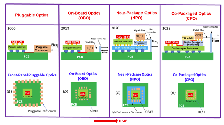

Comments