


2026 OCP APAC Summit | AI Hardware's Next Battlefield Isn't Process Nodes, It's Packaging: Breaking Down ASE CP Hung's “Integration Trilogy”
While everyone is still asking whether the next node is 2 nm or 1.4 nm, ASE Senior Vice President CP Hung, in a recent advanced packaging keynote, effectively rewrote the question: whether AI systems can ship has long ceased to depend on silicon alone — it depends on whether you can integrate compute, memory, optics and power, and still produce at volume. Coming from a major OSAT, this carries different weight — because they are the ones taking on the problem.
CP Hung split advanced packaging into a trilogy of “electrical, optical and power.” Part one: 2.5D moves to fan-out and then to panel level, raising interconnect density and output together. Part two: moving the optical engine from the chassis edge to right beside the compute chip — that is, CPO. Part three: power efficiency, the most overlooked yet highest-leverage piece. All three share one answer: integration. And integration happens to be what Taiwan's OSATs and supply chain do best — and where they should stake their position.
1. Why Now: Demand Isn't Growing, It's Doubling and Doubling Again
CP Hung opened with a number: last year he was talking about semiconductor output potentially reaching $1 trillion; now he has raised that to possibly touching $1.3 trillion this year. There is only one driver — AI. This isn't a gentle business cycle; it shifts the entire supply chain's demand curve upward.
The real point came next. He said every requirement advanced packaging must meet — performance, memory bandwidth, area, power — none is growing gently; all start at 2x and look toward 10x. That's worth pausing on: when demand is “doubling and doubling again,” you can't keep up linearly with existing processes; you have to change how you integrate. That is the fundamental reason packaging has moved from backstage to center stage.
We discussed the same shift in CPO Teardown 2/6: The Paradigm Shift in Photonic Packaging — once the dividends of transistor scaling are used up, the battlefield naturally moves to packaging. CP Hung's talk can be seen as the full version, expanding that shift from photonics to integrating “electrical, optical and power” altogether.
2. Part One: From 2.5D to Panel Level, Solving Density and Output Together
Part one covers the core business — electrical interconnect. The storyline is clear: 2.5D (the familiar CoWoS-type architecture) places the processor, memory and I/O on a silicon interposer, which delivers high density at the cost of a silicon slab that is expensive and hard to scale up. Fan-out then steps in, replacing the costly silicon interposer with redistribution layers (RDL); ASE's line for this is FOCoS (Fan-Out Chip on Substrate).
Next comes FOCoS-Bridge: instead of a full silicon interposer, a small silicon bridge is embedded only where high-density interconnect is needed, with RDL copper layers handling the rest, balancing density and cost. CP Hung's comparison was sharp: traditional flip-chip packaging (FCBGA) has line/space of about 15/15 µm, while the FOCoS route offers about 50x the interconnect density, and FOCoS-Bridge goes even higher. Fine-line substrates reach 3-, 6- and even 12-layer stacks, with line/space down to single-digit microns.
But the most imaginative part of the talk was panel-level packaging. He pointed out the pain point: 2.5D today runs on 12-inch wafers, and after reticle-size limits, each wafer yields only a single-digit number of usable modules; moving to square panels lets the same design yield several times more. This isn't a lab concept — at ECTC this year ASE already presented an approach using a 600mm panel interposer with 300mm panel assembly, which we analyzed fully in ASE's 600mm Panel Interposer Breakdown. When CoWoS capacity is described as the bottleneck holding up the entire AI supply chain, “panel level multiplying output several times” is no longer just a technical question but a capacity strategy question.
3. Part Two: Moving Optics Next to Compute Is What Makes It CPO
Part two is optics. CP Hung's framing is intuitive: traditional pluggable optical modules can only plug in at the chassis edge; the signal must travel electrically from the processor to the edge before converting to light, a path that burns power and limits bandwidth. The essence of CPO (Co-Packaged Optics) is moving the optical engine from the edge to right next to the processor, so electrical-to-optical conversion happens over the shortest possible distance.
He pointed to two implementation paths worth remembering: one uses POP (Package-on-Package) to stack existing photonic chips (PICs), and the other brings 3D stacking into the PIC for true 3D optoelectronic integration. He was also blunt about the sticking point — it's not that it can't be built, it's how to keep it testable and maintain performance and yield after integration. This matches industry consensus: CPO's difficulty was never “whether light can run,” but the unsexy yet fatal engineering details of packaging, testing and serviceability.
Note who is saying this. Optical engine integration used to be the business of optical module makers and foundries; now an OSAT is framing CPO as part of its own packaging roadmap. We broke down this shift of “foundries and OSATs moving from supporting roles to leads” in more detail in CPO Teardown 5/6: The Ecosystem Is Being Reshuffled.
4. Part Three: Power Efficiency, the Underestimated Lever
Part three is the easiest to skip, yet CP Hung spent considerable time on it — power. His logic is pure arithmetic: the power delivery chain from grid to chip loses about 10% to start with; at the scale of AI data centers running hundreds of megawatts, even saving 0.5% translates into significant electricity and cooling costs.
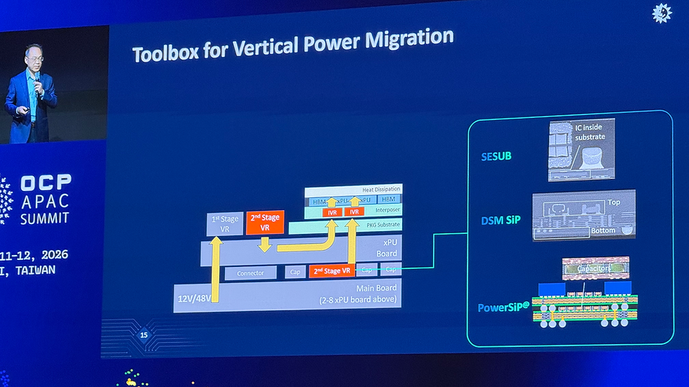
The solution is again integration — pushed into the package. He listed several directions: integrating SMD passives with multilayer substrates, embedding power ICs and inductors directly in the substrate, and using wafer-level RDL for double-sided, smaller-footprint high-voltage power delivery, making power paths shorter with lower losses. Looking outward, there are also medium- and high-voltage power modules outside the package (he mentioned 800V-class module options). In one sentence: power delivery is migrating from the motherboard into the package — an entirely new battlefield for components and design.
Thermal is the hidden cost of all this. When compute, optics and power are all packed into the same package, thermal stress becomes the ceiling on integration — imec quantified the thermal cost of 2.5D/3D CPO across 18 figures, which we covered in imec Breaks Down the Thermal Cost of CPO. The more integrated, the harder to cool — that is the physical limit behind the trilogy that went unspoken, yet cannot be avoided.
5. The Counterargument: Integration Sounds Great, Volume Production Is Another Matter
Here is where to stay sober. CP Hung himself admitted at the end: integrating electrical, optical and power into one system is hard not because of any single technology, but because overall design + yield + thermal stress must all hold at the same time. Flip that honest statement around and you have a risk list.
Panel-level packaging must deal with warpage, yield and a full generational turnover of equipment; CPO must clear optical coupling, testing and serviceability; embedded power must handle heat and reliability. If any link stalls, “integration” turns from a selling point into a cost. And ASE isn't alone on this road — TSMC's CoWoS/SoIC and Amkor's advanced packaging are fighting for the same ground; in Amkor 2026 Q2 Earnings Call we saw a peer list CPO and advanced packaging side by side as growth engines. So the real variable isn't “is the direction right” — that's no longer in doubt — but who can deliver yield and capacity at the same time first.
Conclusion
The value of CP Hung's talk isn't any single technology headline, but that he redefined the competitive threshold for AI hardware: from “whose process is more advanced” to “who can integrate compute, optics and power and still produce at volume”. The trilogy — panel-level packaging for output, CPO for bandwidth and energy, embedded power for efficiency — points to one conclusion: advanced packaging is now a system-level decider, no longer the downstream finishing step of the process.
For Taiwan's supply chain, this is a rare positive signal. The main battlefields of this road — OSAT, substrates, carriers, passives, optical coupling, thermal and test equipment — have Taiwanese companies in almost every slot, and ASE has placed itself squarely in the integrator's seat. As the battlefield moves from “scaling” to “integration,” Taiwan holds a stronger hand. But don't read the signal as blind optimism: none of panel level, CPO or embedded power will be in widespread volume production next year. What really needs tracking is yield figures, the actual adoption timeline for panel assembly, and who gets CPO into a customer's rack first. The direction is set; what comes next is a contest of execution and time.
This article is for technology and industry trend analysis only and does not constitute investment advice.







Comments