


Technical Paper Analysis | Marvell 2.5D Heterogeneous Integration: The Evolution of SiPh Engines and Optical Transceivers
In optical communications, we are living in an era of "speed hunger." As AI compute and data center demand explode, conventional packaging is running into physical limits. The paper analyzed here comes from the Marvell team and details how 2.5D heterogeneous integration can tightly combine electronic components with a silicon photonics (SiPh) engine, tackling the industry's pain points of high-frequency signal loss and power consumption.
Reference
Title: 2.5D Heterogeneous Integration for Silicon Photonics Engines in Optical Transceivers
Authors: Radhakrishnan Nagarajan (Fellow, IEEE), Liang Ding, Roberto Coccioli, et al.
Affiliation: Marvell
Published in: IEEE JOURNAL OF SELECTED TOPICS IN QUANTUM ELECTRONICS, VOL. 29, NO. 3, MAY/JUNE 2023
In-Depth Figure Analysis
1. Defining the Integration Architectures (Fig. 1)
This figure is the foundation for understanding the whole paper. Following the IEEE Heterogeneous Integration Roadmap, Marvell divides architectures into three classes:
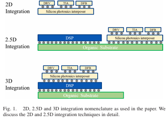
2D integration: Active components (DRV, TIA, DFB laser) are placed side by side on a silicon photonics interposer.
2.5D integration: The 2D optical assembly above is co-packaged with the DSP/ASIC on a high-quality organic substrate.
3D integration: The optical assembly is stacked directly on top of the DSP.
2.5D is today's sweet spot, balancing performance gains with manufacturability.
2. Module Evolution and Energy Efficiency (Fig. 2, 3 & Table II)


These data show a remarkable 20-year track record.
Data rate: From 1G in 2001 to an expected 3.2T CPO in 2024 — three orders of magnitude.
Energy efficiency: Energy per bit dropped from 1000 pJ/bit to 18 pJ/bit.
Pain point: Although efficiency per bit improved, total module power rose from 1W to more than 50W (CPO estimate), putting heavy pressure on thermal packaging.

3. Packaging Paths and Signal Integrity (Fig. 4 & 5)

Marvell simulated three scenarios: conventional PCB wire bonding, 2D optical integration with wire bonding, and a full TSV (through-silicon via) structure.
Frequency response: Fig. 5 clearly shows that wire-bonded packages suffer severe insertion loss and resonances at high frequencies.
TSV advantage: The 2.5D structure using TSVs shows an extremely flat frequency response (solid blue line), which is critical for analog bandwidth at 100 Gbaud and above.
4. 2D Integration Details and Assembly (Fig. 6 - 9)


These figures show what the silicon photonics chip looks like when used as an interposer.
Precision alignment: DFB lasers are placed in etched trenches, and automated equipment (such as the Amicra Nano) achieves high-precision alignment of +/- 5 um.
Thermal resistance: A 300 um-long DFB laser attached to the SiPh interposer was measured at a thermal resistance of 60 +/- 2 degC/W.
5. 2.5D Wafer-Level Process (Fig. 15 & 16)


This is the core technology for commercial volume production.
Via-Last Process: Marvell forms the TSVs from the backside after the silicon photonics wafer is finished. This "build-after" approach is very supply-chain friendly, because most OSATs (outsourced assembly and test providers) already offer mature via-last services, so production is not limited to the few SiPh foundries with TSV capability.
RDL and C4 Bumps: A redistribution layer (RDL) and C4 bumps tightly connect the electro-optical engine to the organic substrate.
6. System-Level Validation (Fig. 19 - 21)
Performance: At 53.125 Gbaud (106.25 Gbit/s), TDECQ was measured at about 2.0 dB, better than the IEEE specification.
Live demo: Fig. 21 shows 16 optical modules integrated with a 12.8 Tbit/s switch chip (Teralynx 7).

Conclusion: The "Standardization" Era of Silicon Photonics
This Marvell paper not only demonstrates technical depth but also points to an industrialization path. Using a via-last TSV flow to integrate heterogeneous components on a silicon photonics interposer solves the parasitic power problem at high frequencies. This matters not only for today's 800G/1.6T modules but is also a necessary step toward CPO (co-packaged optics). Going forward, the line between optical and electronic components will blur further, and packaging technology will become the real performance differentiator.


Comments