


ECTC 2026 | Nokia Bell Labs | Thin-Film Lithium Niobate Hybrid Integration for Co-packaged Optics
Silicon photonic modulators are up against a physical ceiling: RC limits cap their bandwidth at roughly 50–60 GHz, and modulation requires heavy doping, which drives up optical loss. At ECTC 2026, Nokia Bell Labs (with UC Davis) demonstrated for the first time a thin-film lithium niobate (TFLN) Mach-Zehnder modulator hybrid-integrated with a commercial open-collector driver IC via micro-bump flip-chip, forming a transmitter for CPO. The results: Vπ·L as low as 2.3 V·cm, overall electro-optic (EO) bandwidth >45 GHz (the modulator alone exceeds 50 GHz; the ~45 GHz driver IC is the limiter), and a peak driver temperature of ~68°C without forced-air cooling. The key move is using the TFLN PIC as an "electrical interposer" — placing the driver close enough to the modulator (5 mm) to sharply cut parasitics and flatten the EO response. In one sentence: to break through the silicon modulator bandwidth bottleneck, TFLN plus flip-chip hybrid integration is now a validated path for CPO.
1. Background: The Silicon Modulator Bandwidth Bottleneck
The paper comes from Nokia Bell Labs (Murray Hill, New Jersey) and UC Davis, presented at the 2026 IEEE 76th ECTC. AI is pushing data center interconnect bandwidth and energy efficiency to their limits. CPO moves optical I/O next to the XPU to save interconnect power, but the transmitter side faces a materials bottleneck: the silicon photonic modulator.
Silicon modulators rely on a weak electro-optic effect, so they need heavy doping to modulate, which means high power consumption and high optical loss in silicon waveguides, while RC limits cap bandwidth at around 50–60 GHz. Going higher requires a different material. Thin-film lithium niobate (TFLN, thin-film lithium niobate-on-insulator) is widely regarded as the material that can break through this bandwidth bottleneck, thanks to its excellent electro-optic properties and low optical loss.
CPO is won or lost in packaging integration; for context see CPO Is Won in Packaging, Not Optics — John Lau on PIC/EIC Heterogeneous Integration; for the overall evolution of CPO see The Three-Stage Evolution of CPO: From Scale-Out to Scale-Up. This paper contributes the first demonstration of how a TFLN modulator can be integrated with a driver IC for CPO.

2. The Core Question: The Whole Paper in One Sentence
What this paper sets out to prove: can a TFLN Mach-Zehnder modulator and a commercial driver IC be hybrid-integrated via micro-bump flip-chip into a CPO transmitter that delivers high bandwidth, low Vπ and manageable thermals at the same time?
The answer is yes — and the key is using the TFLN PIC as an electrical interposer, bringing the driver within 5 mm of the modulator.
3. Key Figures Explained
3.1 This figure shows the low Vπ and high bandwidth of the TFLN modulator itself

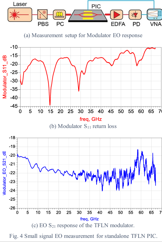
These figures (Fig. 3, Fig. 4) characterize the modulator. The TFLN device uses an x-cut wafer with a 1.6 µm ridge width to stay single-mode, forming a traveling-wave Mach-Zehnder modulator, with on-chip NiCr thermo-optic phase shifters and a termination resistor for the traveling-wave electrodes. Measured Vπ·L = 2.3 V·cm (lower means less power), EO 3 dB bandwidth >50 GHz, and an extinction ratio of ~12 dB (limited by MMI splitter fabrication accuracy). This Vπ and bandwidth are TFLN's intrinsic advantages over silicon modulators.
3.2 This figure shows lower parasitics and a flatter EO response after integration


These figures (Fig. 5, Fig. 6) show the integration benefit. The driver IC alone has ~45 GHz bandwidth and input return loss below -10 dB up to 45 GHz. The key is integration: after flip-chip, the distance from driver output to termination resistor is only 5 mm, impedance matching is good, and ripple in the overall EO response tightens from 5 dB (measured separately) to within 2 dB, with markedly less ringing. The paper notes that the overall EO response is ultimately limited by the driver IC's bandwidth (~45 GHz), not by the TFLN modulator.
Using the TFLN PIC as an "electrical interposer" with the driver sitting right next to the modulator is the core design choice that suppresses parasitics.
3.3 This figure shows the thermals: driver at 68°C, heat spread through micro-bumps into the PIC


These figures (Fig. 8, Fig. 9) present the thermal analysis (simulation plus infrared measurement, agreeing within 3°C). The driver hot spot is the main heat source, peaking at ~68°C (no forced-air cooling); heat is mainly spread into the PIC through high-conductivity copper micro-bumps. Note that the TFLN PIC has a 4.7 µm buried oxide plus several SiO2 passivation layers (6–7 µm of oxide in total). This helps optics and RF, but reduces the efficiency of extracting heat through the backside — a thermal trade-off this architecture has to face.
4. Technical Highlights
The first highlight is the first flip-chip hybrid integration of a TFLN modulator with a commercial driver IC: Vπ·L 2.3 V·cm, EO bandwidth >45 GHz and ~12 dB extinction ratio, with the TFLN PIC designed and fabricated entirely in-house. This moves TFLN from "great material but hard to integrate" to "can be packaged together with a driver in a CPO transmitter."
The second highlight is using the TFLN PIC as an electrical interposer: micro-bump flip-chip tightly couples the driver and modulator within 5 mm, sharply cutting parasitics and tightening EO response ripple from 5 dB to 2 dB — proof that tight integration is itself a performance lever. Next, the team plans to add TSVs inside the PIC to replace RF probes and move to a more complete signal input scheme.
5. Industry Link: How Far from Volume Production, and Who Benefits?
Distance: this is a "first integration demonstration" — EO and thermal performance of the full transmitter have been verified, but two obvious gaps remain: coupling loss of ~8 dB/facet (lensed fibers used directly with no SSC spot-size converter, which is too high), and signal input still via RF probes, which needs to move to in-PIC TSVs. Until these are addressed, it remains some distance from being shippable.
Beneficiaries: most directly, the PIC and materials ecosystem betting on TFLN, along with CPO transmitter designs that treat TFLN as the next-generation high-speed modulation platform. A sober view: TFLN wins on bandwidth and Vπ, but coupling loss, heat dissipation (thick oxide blocks backside heat extraction) and co-design with the driver are all engineering hurdles; moreover, this generation is capped by the ~45 GHz driver IC, so TFLN's >50 GHz is not yet fully exploited. Its value lies in pointing to the path beyond the silicon modulator bottleneck, not in winning this generation.
6. Summary
The one sentence to remember from this paper: to get past the 50–60 GHz bandwidth bottleneck of silicon modulators, Nokia Bell Labs delivered the first CPO transmitter demonstration using a TFLN modulator flip-chip hybrid-integrated with a commercial driver IC — Vπ·L 2.3 V·cm, EO >45 GHz, with the TFLN PIC acting as an electrical interposer to suppress parasitics. For those tracking CPO transmitters, the things to watch: the TFLN route is a contest of "bandwidth/Vπ advantage × coupling loss × heat dissipation × co-design with the driver." This generation proves integration is feasible; coupling and thermals are the next hurdles.
References
Zhixing Lin (UC Davis), Tam Huynh, Ayed Sayem, K.W. Kim et al. (Nokia Bell Labs), "Thin-Film Lithium Niobate Hybrid Integration for Co-packaged Optics," 2026 IEEE 76th ECTC. Nokia Bell Labs, Murray Hill, NJ.
Related Reading
CPO Is Won in Packaging, Not Optics — John Lau on PIC/EIC Heterogeneous Integration: the packaging perspective on transmitter integration
The Three-Stage Evolution of CPO: From Scale-Out to Scale-Up: why CPO needs a higher-bandwidth modulation platform


Comments