


Why Is Silicon Photonics So Hard to Design? The Answer Lies in a Box Called the PDK
Many people assume the hard part of silicon photonics (SiPh) is silicon’s inability to emit light, the laser, or the packaging. But for the people actually designing the chips, the first bottleneck is far more mundane — can you get a box of standard building blocks that the foundry guarantees will yield if you follow the rules. That box is called the PDK (Process Design Kit). It is not software and not a device, but a contract that translates the foundry’s process capabilities into a “design language.” This article explains what a PDK is, what’s inside it, why a silicon photonics PDK is so much harder to build than an electronic one, and why it is actually the foundry’s deepest moat.
1. The Brutal Math of Silicon Photonics: One Tape-Out, Months and Millions
Start with a sense of scale that keeps every silicon photonics designer up at night.
You’ve designed a photonic chip. The only way to verify whether it works is a tape-out — sending the layout to the foundry, running it through the full process, and measuring the real silicon that comes back. Mask costs for a single tape-out run into the millions, and the cycle often takes several months. That means: if you guess wrong on even one detail — a waveguide bent too tightly, a modulator’s high-frequency response off target, a coupler with 2 dB more loss than expected — you wait another round and burn the money again.
The electronic chip world tamed this problem long ago. A digital IC designer doesn’t “guess” what a transistor looks like: every transistor in the library from the foundry has been measured, modeled and guaranteed. The results in the simulator match the silicon that comes back from tape-out closely enough to commit to production.
For silicon photonics to reach volume production, it has to replicate this discipline of “get the answer right on the computer first, then pay for the tape-out.” The core infrastructure that makes this possible is the PDK.

2. Everyone Thinks the Hard Part Is the Laser — It’s Actually a “Construction Manual”
The list of silicon photonics challenges has been repeated endlessly online: silicon doesn’t emit light, III-V lasers must be attached, modulators run into the diffraction limit, fiber alignment must be accurate to the micron. These are all real challenges, and we’ve broken them down in other articles.
But those are “device-level” challenges. What has really kept silicon photonics from becoming like CMOS — where any design house can come in and draw a chip — is the design-level challenge: how can a design team without its own fab be sure the foundry can actually build what it draws?
An analogy makes it clear. To build a house, creativity alone (I want a floating spiral staircase) is useless; you need a construction manual: how much load this rebar can carry, how many days this concrete takes to cure, how far apart beams and columns can be. Without that manual, no matter how beautiful the architect’s drawings, the crew on site can only tell you, “This can’t be built.”
The PDK is the construction manual the foundry hands to designers. It captures what the fab can actually do, how well, and which lines must not be crossed, in a format designers can understand and tools can read. Without a PDK, silicon photonics design is an expensive guessing game; with one, it becomes engineering.
This is also why the fabless model can work in silicon photonics — design houses don’t build fabs; they rely on the foundry’s PDK as a “guarantee of manufacturability.” We break down this business model fully in From Wafer to Royalties: The Silicon Photonics Fabless Business Model Explained; this article focuses on the PDK itself as the core component.
3. What Is a PDK: The Foundry’s “Guaranteed-to-Build LEGO Box”
In one sentence: a PDK is a box of standard optical building blocks provided by the foundry, already verified and guaranteed to be manufacturable on its line, plus a manual that dictates how you assemble them.
Picture a LEGO set. The box holds bricks already molded to precise dimensions (waveguides, splitters, modulators, photodetectors), along with a manual telling you how much spacing to leave between bricks, that bends can’t be tighter than a certain radius, and which bricks can’t be stacked together. You don’t have to injection-mold a new brick yourself — that’s the foundry’s job; your job is to use these guaranteed-compliant bricks to build the photonic chip you want.
The key word is “guaranteed.” Every component in a PDK is not a theoretical value but something the foundry has built on its real process, measured and modeled. Drag a PDK modulator into your design tool, and its behavior roughly matches what comes back from tape-out. That is the magic of the PDK turning “guessing” into “engineering” — it backs your design with the foundry’s credibility.
4. Opening the Box: Component Library, Design Rules and Compact Models
Open the PDK box and you’ll find three layers; without any one of them, it doesn’t count.
Layer 1: Verified Component Library. These are the bricks themselves — waveguides, multimode interference couplers (MMI), grating couplers, splitters/combiners, modulators, photodiodes, tapers and fiber couplers. Each is a standard cell the foundry has already run and confirmed for yield and performance. You don’t design a modulator from scratch; you take it straight from the library.
Layer 2: Design Rules (DRC). This is the manual — line widths, spacing, minimum bend radius, and the definition and stack-up of each layer. It sets the boundary of what is physically manufacturable. Draw a waveguide bend radius too small and light leaks out; place two waveguides too close and they crosstalk. DRC writes these “do-not-cross lines” into rules, and the design tool checks them automatically (design rule check), flagging violations in red. In effect, the foundry’s rules catch your mistakes before tape-out.
Layer 3: Compact Models / Simulation Models. This is the hardest of the three layers and the one that decides life or death. Bricks and rules aren’t enough; you must be able to accurately predict on a computer how these bricks will behave once assembled. A compact model is each component’s “behavioral formula” — its S-parameters (describing the amplitude and phase of optical signals in and out), its response to wavelength, temperature and voltage, and its interfaces to electrical and thermal models. Accurate models mean accurate simulation; accurate simulation means you dare to commit to a tape-out.
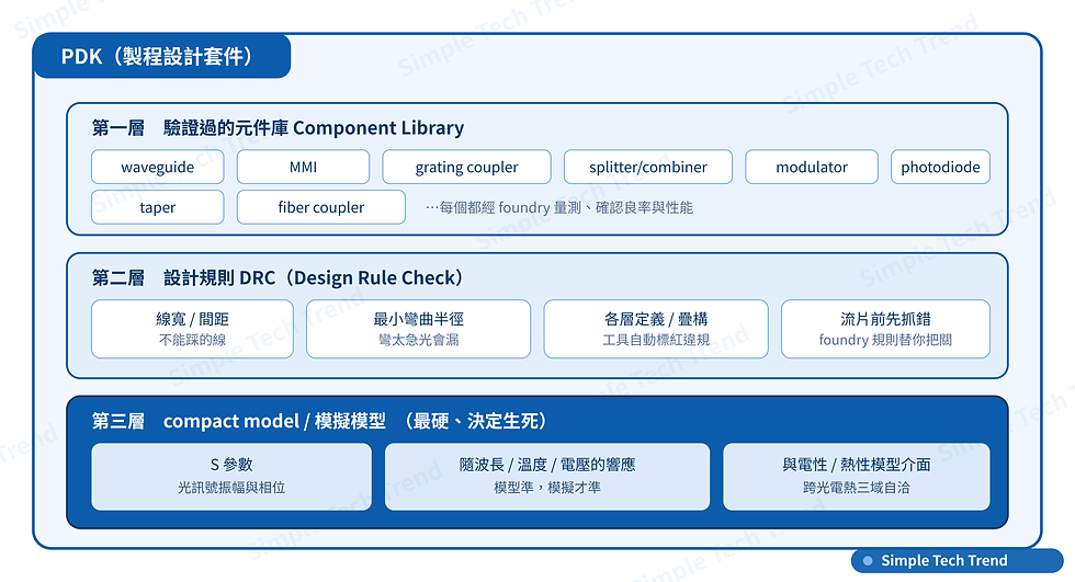
And this third layer is precisely where silicon photonics lags electronics the most — and where it hurts the most.
5. Why Silicon Photonics PDKs Are So Much Harder Than CMOS
CMOS PDKs have been refined for three or four decades and are so mature that designers almost never question them. Silicon photonics PDKs are still catching up. The gap isn’t simply “not enough time”; it’s that the physics of photonics is inherently harder to model than electronics.
First, photonic devices behave continuously and in analog fashion. A transistor is essentially a switch, 0 or 1, and its models are relatively clean. But a photonic modulator’s output is a continuous function of wavelength, voltage, temperature and process variation; getting it accurate across the whole spectrum and temperature range makes the model an order of magnitude more complex.
Second, extreme sensitivity to process variation. A waveguide width off by just a few nanometers changes the phase light accumulates as it travels, and the behavior of an entire interferometric device can drift. Electronic chips tolerate such nanometer-scale errors far better; in silicon photonics, a few nanometers can throw everything off. Compact models must therefore capture process variation too, which raises the difficulty sharply.
Third, models must span three physical domains — optical, electrical and thermal. For a single modulator, you must compute its optical response, its high-frequency electrical behavior (RF loss, impedance, skin effect) and the thermal wavelength drift once it heats up. All three domains must be self-consistent in one model — a complexity electronic PDKs rarely face. This is also why many silicon photonics compact models were long stuck at 25 Gbaud: the high-frequency electrical behavior wasn’t modeled accurately. We cover how this tough problem was cracked in a dedicated paper review, Silicon Photonics Transceiver Design Finally Runs at 64 Gbps in a Standard Circuit Simulator.
Fourth, the scales differ by four orders of magnitude. The optical carrier frequency is about 193 THz (1550 nm wavelength), while electrical signals are only tens of GHz — a 10,000× difference. Handling this scale gap in a single simulator requires mathematical techniques like “equivalent baseband models” that shift away the optical carrier frequency and keep only the slowly varying envelope; otherwise the sampling rate would explode beyond computability.
Fifth, there is no standardization yet. Electronic PDKs have mature formats and ecosystems; switching foundries leaves the design flow largely the same. In silicon photonics, component naming, model formats and tool interfaces still vary from vendor to vendor, locking designers into specific platforms and forcing them to start over when they switch.
Stack these five factors together and you see why the “silicon photonics PDK” remains a battleground where foundries and EDA vendors are investing heavily, yet no one has fully solved it.
6. Where the Moat Lies: PDK + EDA Lock-In and Foundry Positioning
At this point, STT wants to offer an industry-level takeaway: the PDK isn’t just technical documentation — it’s the foundry’s deepest and quietest moat.
The logic goes like this. Once a design team picks a foundry’s PDK, builds its entire design flow on it, trains a group of engineers fluent in it, and gets its first working silicon, that team is “stuck.” Switching foundries means redoing the whole component library, models and design experience. That switching cost is the source of the foundry’s pricing power. And the PDK only works when tied to EDA tools — Synopsys OptoCompiler, Luceda IPKISS, Keysight ADS — creating a two-layer “foundry × EDA” lock-in ecosystem. Whoever has the most complete PDK ecosystem and the smoothest EDA integration attracts the most designers.
The current positioning looks roughly like this:
GlobalFoundries’ Fotonix platform is widely regarded as one of the most complete silicon photonics PDKs with the most mature ecosystem, but it has also been called out by academia — its silicon modulator optical link simulation only goes up to 26.5 Gbaud, lacks noise modeling, and most details are undisclosed, which falls short for next-generation 800G/1.6T systems. GF’s recent partnership with Cadence on “photonic-native” compact models aims to close that gap; we cover this paradigm shift in GF and Cadence Team Up to Drive Photonic-Native Compact Models.
Tower Semiconductor takes a different path — fabless players like OpenLight integrate their PDK directly into Luceda IPKISS on top of Tower’s line, creating a division of labor where “design houses draw with the OpenLight PDK and hand off directly to Tower’s process.” TSMC enters through its COUPE platform, redefining its silicon photonics PDK from the circuit designer’s perspective (we discussed this in TSMC Enters the Silicon Photonics Era: Three Key Innovations from a Circuit Designer’s Perspective). Samsung Foundry is pushing full volume production on a 300mm silicon photonics platform, emphasizing a one-stop offering from PIC to CPO and challenging the first two head-on.

But this moat has cracks. Academia has started building open-source, verifiable, cross-foundry compact model libraries — for example, an open-source Verilog-A photonic model library from a Yokohama National University team, validated all the way to 64 Gbps signaling with every detail made public, directly challenging the assumption that a PDK must be tied to a foundry and closed-source. Whether this force loosens foundry lock-in is a signal worth watching over the next few years.
Conclusion
For silicon photonics to move from “pretty lab demos” to “millions of units shipping in data centers,” what’s missing has never been just better modulators or brighter lasers, but a design discipline that lets everyone “get the answer right on the computer first, then pay for the tape-out.” The PDK is the foundation of that discipline — it backs designs with the foundry’s credibility and turns guessing into engineering.
So the next time a foundry announces “another silicon photonics PDK upgrade,” don’t dismiss it as boring tech news. However accurate the PDK is, that’s how far silicon photonics can scale in volume; whoever the PDK locks in is who pays the toll on this supply chain. This unassuming box of building blocks is the quietest — and most decisive — move in the silicon photonics war.
Related Reading
From Wafer to Royalties: The Silicon Photonics Fabless Business Model Explained: the PDK is key to whether fabless can work; this piece breaks down the full “design → foundry → royalties” business model
Silicon Photonics Transceiver Design Finally Runs at 64 Gbps in a Standard Circuit Simulator: how the toughest layer, the compact model, was cracked — a paper review of an open-source Verilog-A model library
OFC2026 | GF and Cadence Team Up to Drive Photonic-Native Compact Models: a paradigm shift in silicon photonics design simulation — how the foundry and EDA fill the high-frequency modeling gap
Silicon Photonics Optical Modules Explained: Six Interfaces, Core Components and Industry Examples: first understand how the components in a PDK connect inside a real optical module


Comments