


ECOC 2026 | 1.6T Has Just 4 Years to Hit 10 Million Units: Lumentum Opens Its Volume-Production Books — 49% of Module Power Goes to the DSP, and Only 24% of the DSP Does Compute
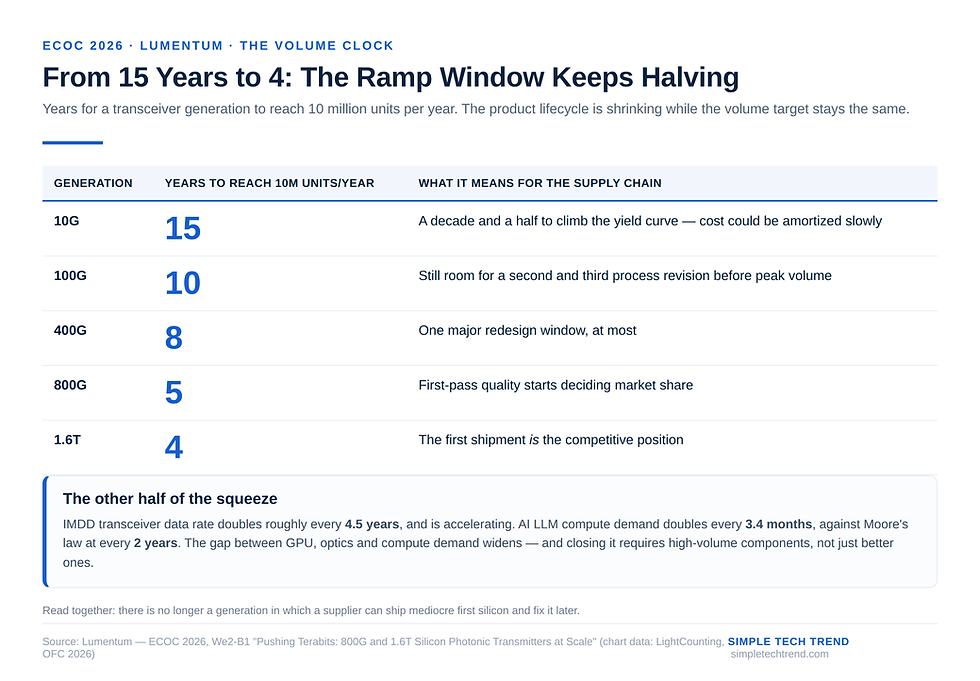
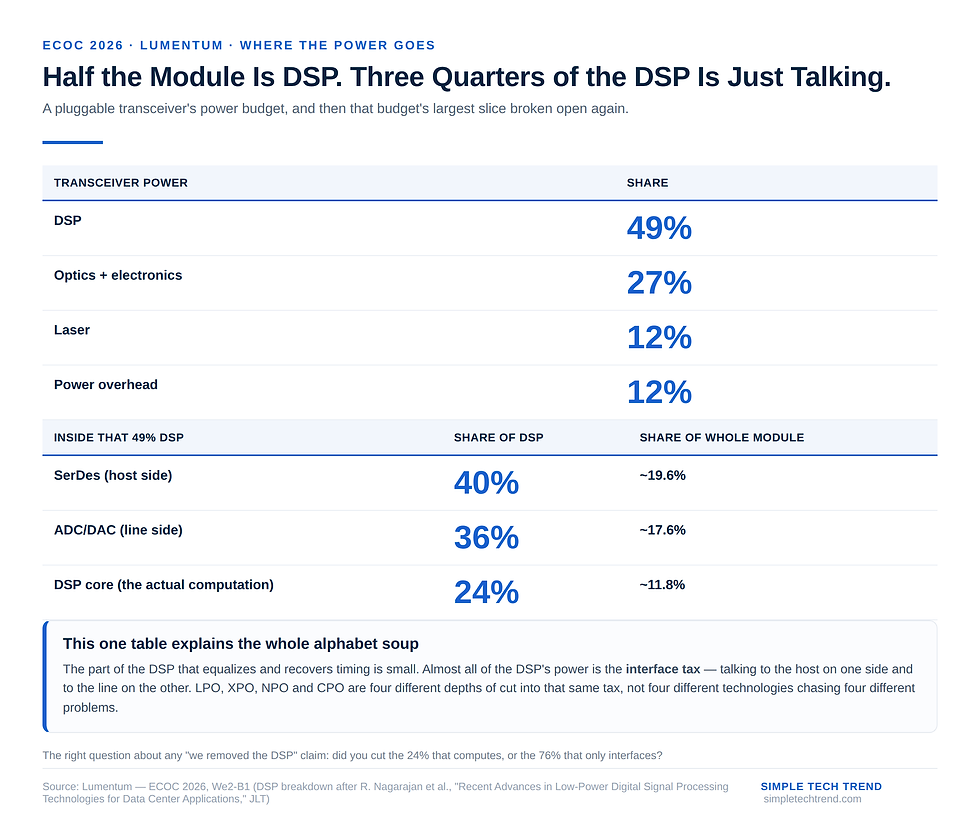
This is a talk that puts hard numbers on "why this generation is different." Lumentum's Erman Timurdogan put two sets of figures on the table. The first: from 10G to 1.6T, the time it takes a data rate to go from launch to 10 million units shipped per year has shrunk from 15 years to 4; the second: in a pluggable module's power budget, the DSP accounts for 49%, and the core inside the DSP that actually does computation is only 24% of that — the other 76% is SerDes (40%) and ADC/DAC (36%), purely talking to the outside world. Together, these two numbers are the entire motivation behind the LPO/XPO/NPO/CPO wave. And his next-generation targets are just as hard: LPO/XPO/NPO aim for <10 pJ/bit, with switch radix growing from 512 to 1024 (200G/lane); CPO aims for <5 pJ/bit, going slow-and-wide, with radix potentially reaching 4096 (50G/lane). Yet the most practical part of the talk wasn't about performance — it was about testing: he said bluntly that the bottleneck in automated functional testing of optics is things like "plugging in fibers and cleaning fibers."
1. The "years to 10 million units" chart is the one slide everyone should copy
The talk opened with two layers of macro context. The first is compute: citing OpenAI's AI and Compute study, the slide noted that Moore's Law doubles every two years, while AI LLM compute demand doubles every 3.4 months; next to it, Kaplan's scaling-law curve (L = 2.57·C^−0.048) adds that "more compute improves the accuracy of AI output" — in other words, this demand isn't going to stop on its own.
The second layer is the key one. The x-axis is the data-rate generation; the y-axis is "how many years it took from first shipments at that rate to reach 10 million units shipped per year":
10G: years to reach 10 million units/year — 15 years
100G: years to reach 10 million units/year — 10 years
400G: years to reach 10 million units/year — 8 years
800G: years to reach 10 million units/year — 5 years
1.6T: years to reach 10 million units/year — 4 years
The left chart on the same slide shows that IMDD optical module data rates double roughly every 4.5 years — and the pace is accelerating.
Put together, the message is clear: product lifecycles are shrinking, yet volumes must climb higher in the same span of time. The slide's conclusion is blunt — the gap between GPU, optics and compute demand is widening, and closing it requires high-volume components.
For the supply chain, this is a structural shift in pressure: in the past, a generation gave you a decade to slowly ramp yield and amortize cost; now you have four years. The quality of your first shipments is almost the whole of your competitiveness for that generation.
2. Where the module's power goes: half in the DSP, and three-quarters of the DSP just talks to the outside world
Next, he tore down a pluggable module. On the left is the physical teardown — circulator, mux/demux, laser, DSP; the two pie charts on the right are the core of the talk.
Pie chart one: power distribution across the whole transceiver.
DSP: share 49%
Optics + electronics: share 27%
Laser: share 12%
Power overhead: share 12%
Pie chart two: breaking that 49% DSP down further.
SerDes (host side): share 40%
ADC/DAC (line side): share 36%
DSP core (the computing part): share 24%
The speaker's point on stage was clear: the DSP core that actually does equalization and clock recovery is quite small. Most of the DSP's power goes to "interfacing with the outside world" — host-side SerDes and line-side ADC/DAC.
Multiply the two pie charts: SerDes accounts for about 19.6% of the whole module, ADC/DAC about 17.6%, while the DSP core actually doing computation is only 11.8% of the module.
This breakdown is the entire rationale behind the LPO, XPO, NPO and CPO alphabet soup. Every one of these approaches is essentially doing the same thing — cutting away part of that "interface tax." LPO removes the DSP, XPO and NPO move the optics next to the ASIC, and CPO co-packages outright. The only differences are where the cut is made and how deep it goes.
It also echoes the debate we covered in ECOC2026 | Fast-narrow vs. slow-wide argued for three hours, but no one defined "slow" first: the real dividing line is 448G — the pJ/bit numbers people quoted differed by 54×, largely because there was no consensus on whether this interface tax was counted.
3. The 800G–1.6T DR8 PIC has only four kinds of components
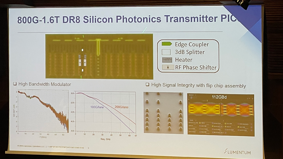
He then showed the layout of the in-production 800G–1.6T DR8 silicon photonics transmitter PIC, and the legend for the entire chip has only four items: edge coupler, 3 dB splitter, heater, and RF phase shifter.
The simplicity is deliberate. An InP laser couples in from the edge, a 3 dB splitter divides it into two arms, each arm is modulated by an RF phase shifter, and the two interfere back together to produce the amplitude modulation IMDD needs — a Mach-Zehnder. The chip has no microrings, no tunable filters, and no resonant cavities that need locking.
On performance, he offered two pieces of evidence:
Modulator bandwidth: the EO S21 curve remains usable out to around 60 GHz, and the chart on the right overlays the channel responses for 100G/lane and 200G/lane — at 67 GHz the 200G/lane curve is noticeably flatter than the 100G/lane one, meaning the design already leaves margin for 200G/lane.
Signal integrity: a photo of the flip-chip bump array, alongside a 112 GBd eye diagram.
What Taiwanese suppliers should note here is the choice itself: for the 1.6T generation, Lumentum is betting on "simple structure + flip-chip packaging," not "complex structure + advanced algorithms." The reason is in the next section — the bottleneck for volume production isn't performance, it's variation.
4. Coupling efficiency: Gen1 to Gen2 halves FAU loss, plus linearity up to 220 mW
This is, in my view, the most engineering-dense slide of the talk.
Three coupling-loss numbers:
SSC → laser (dual lens): edge coupler insertion loss < 0.8 dB
Gen1 SSC → fiber array unit (FAU): edge coupler insertion loss < 1.8 dB
Gen2 SSC → fiber array unit (FAU): edge coupler insertion loss < 0.9 dB
In a single generation, FAU coupling loss dropped from 1.8 dB to 0.9 dB — a full half. The coupling-efficiency curve over 1260–1360 nm on the left shows that Gen2's measured values (about −0.8 to −0.9 dB/facet) are not only lower, but the whole curve is much flatter — Gen1 degrades noticeably beyond 1320 nm, while Gen2 holds up all the way to 1360 nm.
The slide's annotation reads: efficiency comes from a predictable, seamless interface — that is where manufacturing margin comes from. The key word is "predictable," not "low."
The second number is linearity. The chart on the right plots the on-chip monitor photodetector reading against InP laser input power: it is a straight line from 0 to 220 mW, with the reading climbing linearly to about 6.5 mA. The slide spells it out — "maintaining linearity at high input optical power is key to reducing laser count."
In plain terms: if the chip can take 220 mW without saturating or distorting, you can feed more channels from one laser instead of pairing a laser with every channel. Lasers account for 12% of module power, and a sizable share of cost and reliability risk — using fewer of them is a direct competitive advantage. This lines up exactly with the conclusions of the light-source workshop at the same ECOC, which we covered in ECOC2026 | Data centers need billions of lasers, but the bottleneck is the 5 minutes it takes to "attach" them.
The next slide is a wafer map: wafer-level testing of a typical 1.6T DR8 shows loss variation across the full wafer of < 0.5 dB (color scale ±0.25 dB). Beside it, 2×DR4 wafer starts from 2024 to 2025 trace an upward-curving line. The slide's conclusion: scaling silicon photonics products requires low-variation components and wafer-level distribution data.
5. What really holds up volume production is testing — specifically, "plugging in fibers"
This is, in my view, the most underrated part of the talk — and the most useful for Taiwanese suppliers.
When discussing manufacturing challenges, the speaker raised several points, none of them about performance: the optics industry relies heavily on epoxy and active alignment — the biggest difference from IC manufacturing, and the ceiling on throughput. Reliability qualification requires 2,000 hours of testing or more, and switching a single component supplier can mean running it all again.
Then came the bluntest line: automated functional testing of optics is time-consuming, and the bottleneck is often "plugging fibers in at the test station" — cleaning fibers, inserting fibers, assembly, structural testing first and functional testing after.
Lumentum's path forward has two steps:
Step one: wafer-level testing with vertical couplers. The slide shows box plots of tap ratio across channels A–D and die-level test results for a SiPho-integrated MUX. But it also honestly flags the limitation: vertical couplers offer high throughput, but can only test a single polarization and a single passband. Then it leaves an open question: "So how do you test coherent or CWDM PICs?"
Step two: next-generation wafer-level edge-coupling test. This is their answer: use the silicon photonics dicing trench so a standard FAU can couple in from the edge and test at the wafer stage. The slide shows a photo of the WLT edge-coupler FAU optical probe, plus a mode-field profile with FWHM > 6 µm, and six alignment heat maps on the right.
What this means: turning "must be diced and packaged before testing" into "testable on the wafer." For a generation that has only four years to go from zero to 10 million units, this isn't an efficiency gain — it's the price of admission: the earlier bad dies are screened out, the less of the expensive, slow active alignment and packaging labor downstream is wasted.
For Taiwan's supply chain, this is the most concrete takeaway: the opportunity here isn't in silicon photonics itself — it's in probe cards, FAU optical probes, wafer-level alignment fixtures, and dicing and inspection equipment that can handle dicing trenches. None of this is epitaxy or foundry business; it's equipment and precision-component business.
6. Two numbers for the next generation: <10 pJ/bit and <5 pJ/bit
The final section returns to the roadmap, and this chart gives very clear coordinates.
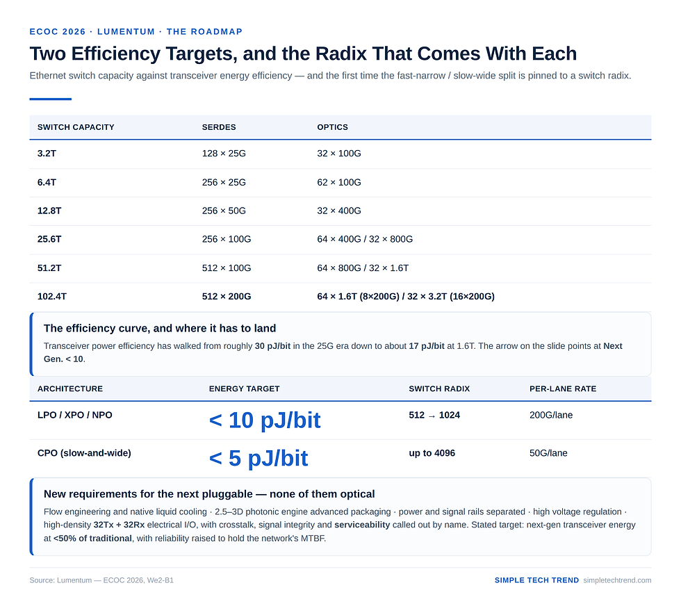
On the left is a dual-axis chart: Ethernet switch capacity (3.2T all the way to 102.4T) against optical transceiver energy efficiency (pJ/bit), on a 2016–2026 timeline. The efficiency curve falls from about 30 pJ/bit to 17 pJ/bit, with an arrow pointing to "Next Gen. < 10."
Each capacity step is labeled with its SerDes and optics configuration — worth writing down:
3.2T: SerDes 128 × 25G; optics 32 × 100G
6.4T: SerDes 256 × 25G; optics 62 × 100G
12.8T: SerDes 256 × 50G; optics 32 × 400G
25.6T: SerDes 256 × 100G; optics 64 × 400G / 32 × 800G
51.2T: SerDes 512 × 100G; optics 64 × 800G / 32 × 1.6T
102.4T: SerDes 512 × 200G; optics 64 × 1.6T (8×200G) / 32 × 3.2T (16×200G)
The two concluding lines underneath are the real judgment:
LPO, XPO and NPO target <10 pJ/bit, with switch radix growing from 512 to 1024 (200G/lane).
CPO targets <5 pJ/bit via the slow-and-wide route, with potential switch radix of up to 4096 (50G/lane).
These two lines tie the "fast-narrow vs. slow-wide" yardstick to switch radix for the first time. 1024 lanes at 200G/lane and 4096 lanes at 50G/lane deliver total bandwidth of the same order of magnitude, but the difficulty in packaging, shoreline, power and reliability is completely different. This is exactly what everyone at this ECOC was really arguing about — we broke down the full structure of this yardstick in After copper can't keep up with AI: seven paths for scale-up optical interconnect, and two ways to live with the wall each one hits.
The speaker's list of new requirements for next-generation pluggables is likewise entirely system-level — not one item is "make the optics better": flow-path engineering and native liquid cooling, advanced packaging for 2.5–3D photonic engines, separation of power and signal rails, high-voltage regulation, and high-density electrical I/O at 32Tx+32Rx (crosstalk, signal integrity, serviceability).
Note that last word: serviceability. It's the same signal as Huawei ranking "serviceable" ahead of "power-saving" at the same ECOC — when module density gets this high, whether it can be repaired becomes as important a spec as how much power it saves.
The conclusion slide also carries a hard target: next-generation transceivers (XPO/NPO/CPO) aim for <50% of the energy of conventional solutions, and reliability must improve to maintain MTBF in new networks.
7. Conclusion
Placed in the context of ECOC 2026, Lumentum's position is distinctive: while others argue about "which path to take," it's saying "whichever path you take, you first have to clear the volume-production hurdle."
For Taiwan's supply chain, three concrete takeaways:
First, that "4 years" chart belongs on the conference-room wall. What it changes isn't the technology roadmap, but the basic assumptions of project scheduling. The old rhythm of "sample first, ramp yield slowly, start making money in year three" no longer holds for 1.6T — within four years this generation must be at full volume, and the next one is already knocking. Whoever ships high-yield, low-variation parts from the very first batch captures those four years.
Second, the 49%/24% breakdown is the right denominator for evaluating any "DSP-less" approach. When someone claims a solution saves so much power, the first question should be: are you cutting the DSP core's 24%, or the 76% that is SerDes plus ADC/DAC? Cutting the former means almost nothing; cutting the latter is what counts. That's also why CPO dares to claim <5 pJ/bit while LPO/XPO/NPO only claim <10 — the cuts go to different depths.
Third — and most underrated — test equipment and fixtures are the hidden opportunity of this cycle. The speaker said in his own words that the bottleneck is "plugging in and cleaning fibers," and their solution is to move FAU optical probes onto the wafer and use dicing trenches for edge-coupling tests. This is a position where standards aren't set, players are few, and demand is being forced by a four-year time crunch. For Taiwanese suppliers, the barrier to entry is lower and the time window clearer than squeezing into yet another silicon photonics chip-design slot.
Verdict: This talk announced no new technology, but it redefined the difficulty of the 1.6T generation from "can you build it" to "can you build ten million identical good ones within four years." When the DSP core is only 12% of module power, when FAU coupling loss halves in one generation, when the test bottleneck is plugging in fibers — it all says the same thing: competition in silicon photonics is no longer an optics competition, it's a manufacturing competition. And manufacturing competition is exactly the kind Taiwan's supply chain should understand best.
This article is for technology and industry trend analysis only and does not constitute investment advice.
Related Reading
ECOC2026 | Fast-narrow vs. slow-wide argued for three hours, but no one defined "slow" first: the real dividing line is 448G: the route debate at the same ECOC, and why the pJ/bit figures people quoted differed by 54×
ECOC2026 | Data centers need billions of lasers, but the bottleneck is the 5 minutes it takes to "attach" them: the capacity bottleneck in light sources and packaging alignment — the flip side of this article's motivation to reduce laser count



Comments