


ECTC 2026 | Dai Nippon Printing | High-Density Polymer Waveguide Integration on Glass Substrate for CPO
At ECTC 2026, Dai Nippon Printing (DNP) used imprint lithography to integrate polymer optical waveguides on a glass substrate at a 10 µm pitch, the fine pitch that high-density GPU-to-GPU optical interconnect needs. But the real point of this paper is a design rule: the price of density is paid in “index contrast (Δ).” The narrower the pitch, the worse the crosstalk between adjacent waveguides; DNP showed with both simulation and measurement that as long as the relative index difference between core and cladding reaches Δ≥2.3%, crosstalk at a 10 µm pitch drops below −30 dB (measured: −32.3 dB). On reliability, after HTS at 150°C for 500 hours, Δ fell only from 3.02% to 2.87%, with no impact on single-mode transmission or bending loss. In one line: whether high-density polymer waveguides are feasible depends on whether your index contrast is high enough.
1. Background: polymer waveguides on glass, built for GPU interconnect
This paper from Dai Nippon Printing (DNP, Chiba, Japan) was presented at the 2026 IEEE 76th ECTC. AI and IoT are blowing up data center traffic; today’s pluggable optical modules place electro-optical conversion at the edge of the organic board, where long electrical traces create loss and power bottlenecks. CPO solves this by pulling optics closer to the compute chip. DNP’s concept: integrate polymer optical waveguides on a large-area glass substrate, with multiple GPUs sharing one glass panel and high-bandwidth GPU-to-GPU and package-to-package links running over optical interconnect.
We broke down the benefits of glass as a substrate (low CTE, flatness, electrical and optical coexistence) in Glass substrates are no longer PowerPoint technology: why the TGV race comes together in 2026; DNP adds the “polymer optical waveguide on glass” layer, a different facet of the same material route as Polymer waveguides withstand +20 dBm for six hours.

2. The core problem: the whole paper in one sentence
The problem this paper solves: when imprint lithography is used to make polymer waveguides at a 10 µm pitch, how do you suppress crosstalk between adjacent waveguides, and can the material hold up on reliability?
The answer: raise the relative index difference (Δ) between core and cladding.
3. Key figures, one by one
3.1 This figure shows that “a 10 µm-pitch core pattern can be made”

This figure (Fig. 2) is an SEM: a 10 µm-pitch core pattern made by imprint lithography (top view) and a cross-section with a thin residual layer. Imprint lithography inherently leaves a thin residual layer between the mold and the substrate, a common issue with imprinting. DNP uses a squeegee to scrape off excess core material, significantly reducing residual layer thickness; the thinner the residual layer, the lower the crosstalk.
3.2 This figure shows that “crosstalk is suppressed with index contrast”


This set of figures (Fig. 3 simulation, Fig. 5 measurement) is the core of the paper. Crosstalk is defined as the output intensity difference between the excited waveguide and its neighbor. Simulation (BPM) shows that with −30 dB as the threshold, the minimum usable pitch is 50 µm at Δ=0.5%, 20 µm at Δ=1.0%/2.0%, and only Δ=3.0% reaches 10 µm. Measurements (Δ=0.4%/1.3%/2.3%) agree: Δ=0.4% needs 30 µm, Δ=1.3% needs 20 µm, and only Δ=2.3% keeps crosstalk within the threshold at a 10 µm pitch, measured at −32.3 dB.
The conclusion is hard-edged: the higher the index contrast, the narrower the usable pitch. For 10 µm density, Δ must be at least 2.3%. The same high contrast also keeps bending loss acceptable at a small bend radius (1 mm); simulation shows bending loss exceeds 0.1 dB only when Δ drops below 1.4%.
3.3 This figure shows “how much index contrast drops after high temperature”: reliability
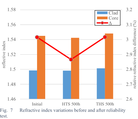
This figure (with HTS/THS data) measures material reliability. Polymer waveguides typically show larger refractive index changes than glass or silicon under high temperature and humidity, causing mode mismatch and scattering. DNP ran HTS at 150°C and THS at 85°C/85%RH per JEDEC. Result: after 500 hours of HTS, the relative index difference fell only from 3.02% to 2.87% (down 0.15%). Evaluated from both the single-mode condition (V-parameter) and bending loss, this change doesn’t affect transmission; bending loss only breaks 0.1 dB once Δ falls below 1.4%, far from 2.87%.
4. Technical highlights
The first highlight is clearly quantifying the design rule that “high density = high index contrast”. With both simulation and measurement as evidence, DNP gives the minimum usable pitch for each Δ, effectively handing future designers a lookup table of “how narrow you want to go, how high Δ must be.”
The second highlight is the imprint lithography + squeegee process for reducing the residual layer, which suppresses the residual-layer crosstalk that plagues imprinting, plus verification that Δ remains sufficient after 500 hours at high temperature, giving polymer waveguides on glass practical reliability.
5. Industry links: how far from volume production, and who benefits?
Distance: this is at the “characterization and reliability verification” stage. The 10 µm pitch, −32.3 dB crosstalk, and 500-hour reliability all pass, but the paper honestly flags its limits: crosstalk rises as the fine-pitch section gets longer, and index contrast has a physical ceiling. There is still a system integration gap before panel-level GPU interconnect reaches volume production.
Beneficiaries: most directly, the glass substrate + polymer waveguide material/imprint equipment chain (DNP itself built its business on printing and imprint know-how); next, packaging and system makers looking to build large-area glass optical interconnect boards. This route and Corning’s glass optical waveguides (ion exchange) are two material answers to “building optical paths on glass”: one uses waveguides in the glass itself, the other lays polymer on top of glass, each with its own cost and reliability trade-offs.
6. Conclusion
The line to remember from this paper: whether high-density polymer waveguides can reach 10 µm depends on whether your index contrast is high enough. DNP used Δ=2.3% to push crosstalk to −32.3 dB and showed Δ is still sufficient after 500 hours at high temperature. For anyone tracking CPO optical redistribution, the thing to watch is that the competitiveness of the polymer waveguide route lies in three material parameters, “index contrast × residual layer control × Δ stability at high temperature,” not just the pitch number.
References
Takuya Kitainui, Yujiro Saito, Naoki Fukuda, Kenichi Ogawa, "High-Density Polymer Waveguide Integration on Glass Substrate for CPO," 2026 IEEE 76th ECTC. Dai Nippon Printing Co., Ltd., Chiba, Japan.
Related reading
Glass substrates are no longer PowerPoint technology: why the TGV race comes together in 2026: the electrical value of glass as a substrate
Technical article analysis | Polymer waveguides withstand +20 dBm for six hours: high-power reliability of the polymer waveguide route


Comments