


ECTC 2026 | imec | Wafer-to-Wafer Hybrid Bonding Technology with 200nm Interconnect Pitch
At ECTC 2026, imec pushed the interconnect pitch of wafer-to-wafer (W2W) hybrid bonding down to 200 nm — the densest 3D-stacking interconnect node to date. But the real message of this paper is not “it shrank again”; it is “at this scale, the bottleneck has changed hands.” At a 200 nm pitch, yield is no longer decided by bonding itself but by two things further upstream: overlay accuracy and CMP planarity. imec's data is hard-edged: to reach ~90% electrical yield at a 250 nm pitch, 80% of the dies across the wafer must have overlay errors below 50 nm. Holding that line took an EVG NT3 aligner to push overlay to sub-100 nm, plus lithography pre-compensation that cut the non-linear residual by 3× (60→20 nm). Yet at a 200 nm pitch (100 nm pads), yield on large chain structures collapses from 65%+ at 250 nm to 20% — copper corrosion, lithography and electroplating fill all hit their bottlenecks at once. In one sentence: as 3D stacking moves below 200 nm, the deciding factor shifts from “bonding” to “overlay + CMP + pad design.”

1. Background: the team pushing 3D-stacking interconnect to 200 nm
This paper comes from imec in Leuven, Belgium, and its authors are the core W2W hybrid bonding team — Van Huylenbroeck, Eric Beyne and others. Beyne is the one who presented sub-2 µm Cu/SiCN hybrid bonding at IEDM in 2017; the same team has driven this roadmap all the way from 2 µm down to 250 nm. It was published at the 76th IEEE ECTC in 2026.
Why does it matter now? Because the density demands of AI compute are pushing 3D stacking to the limit: logic-on-logic, future HBM stacks and heterogeneous chiplet integration all rely on ever-denser die-to-die interconnect. Hybrid bonding (direct copper-to-copper bonding, bumpless) is the highest-density process on this path: the smaller the pitch, the more interconnects per unit area, and the better the bandwidth and energy efficiency. In this paper imec demonstrates an “effective interconnect pitch of 200 nm” and shows high electrical yield on daisy-chain structures.
How does this connect to optical communications? The end-state CPO scale-up architecture — switch ASIC and optical engine sitting on the same substrate, stacked via W2W hybrid bonding — is built on exactly this process, as we noted in The great shift in optical packaging (Part 2): the three-stage evolution of CPO. Pushing hybrid bonding pitch down is the same as pushing the possibilities of 3D integration up.

2. The core question: the whole paper in one sentence
The question this paper tackles is: at a 200 nm interconnect pitch, which upstream processes stand in the way of high, stable electrical yield for W2W hybrid bonding, and how tightly must each one be controlled?
The answer boils down to three things: overlay must be < pitch/4; CMP must deliver atomic-level planarity with precise control of pad dishing and erosion; and effective copper pad density must be kept below 25%.
3. Key figures, one by one
3.1 This figure shows the clever switch from a square to a hexagonal pad layout

This figure (Fig. 2) compares square and hexagonal pad grids. At the same pad area density, a hexagonal grid gives uniform pad spacing in every direction and a larger overall spacing. More uniform spacing → better planarity after CMP → fewer voids at the bonding interface. It looks like a minor choice but actually determines the underlying planarity — the details that decide yield start with the layout.
3.2 This figure shows that overlay accuracy and yield are locked in a linear relationship
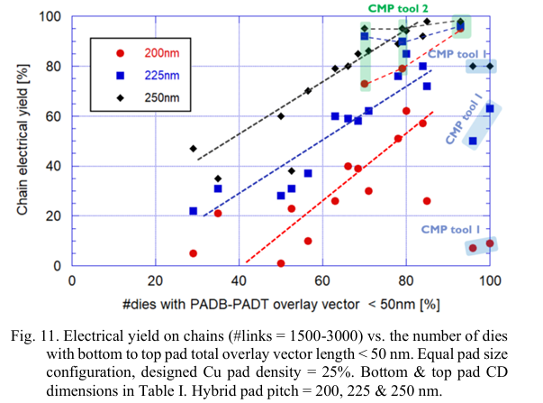
This figure (Figs. 11–13) plots electrical yield against “the fraction of dies with pad-to-pad overlay error < 50 nm.” The conclusion is very firm: overlay accuracy and electrical yield show a clear linear relationship, and at the same overlay a larger pitch gives higher yield. To reach about 90% yield at a 250 nm pitch, at least 80% of the dies across the wafer must have an overlay vector length < 50 nm; shrinking to 225 or 200 nm requires even better overlay.
That is why imec emphasizes aligner upgrades: the EVG GEMINI with the NT2 aligner achieves overlay < 200 nm, while the new NT3 face-to-face aligner pushes overlay to sub-100 nm, raising the fraction of dies with a pad-to-pad vector < 50 nm from ~60% to about 80%.


3.3 This figure shows lithography pre-compensation cutting the non-linear residual by 3×

This figure (Fig. 9) shows the key process trick. Overlay error splits into linear components (translation, rotation, scaling) and non-linear components (wafer distortion residuals). Most of the non-linear residual is a wafer-to-wafer repeatable fingerprint — and since it is repeatable, it can be pre-compensated in the hybrid pad lithography step before bonding (after averaging, 50% of the residual is assigned to the bottom pads and 50%, mirrored, to the top pads). The result: the 95th-percentile residual vector length drops from 60 nm to 20 nm, a full 3×.
The essence of this trick is “absorb the repeatable error” — not by making the tool perfect, but by measuring the systematic fingerprint and correcting it in reverse through lithography.
3.4 This figure shows that 200 nm is a yield cliff

This figure (Fig. 15) measures yield on large interconnect chains (450,000 to 900,000 links). Pitches > 300 nm yield 100%; 250 and 225 nm reach about 65% or more; but at 200 nm (100 nm pads) yield collapses to 20%. imec openly says failure analysis is still under way; suspected causes are pad corrosion (worse for small pads), sub-optimal lithography conditions for small-pad CD, or copper electroplating fill issues.
This is the most honest figure in the paper — it doesn't claim 200 nm is already won, but draws the cliff instead: at this pitch, several upstream problems approach their critical limits at the same time.
4. Technical highlights: two points truly worth remembering
The first highlight is the methodology of “absorbing repeatable error with lithography pre-compensation”. Once hybrid bonding reaches nanometer-level overlay, tool precision alone can't keep up; imec's answer is to treat the non-linear residual from wafer distortion as a measurable, repeatable fingerprint and correct it in reverse with lithography before bonding, squeezing the 95th-percentile residual from 60 nm to 20 nm. This is the “use design/litho to compensate for process” mindset, and it is more effective than simply throwing more hardware at the problem.
The second highlight is clearly identifying the yield bottleneck as three things — overlay, CMP and pad density — rather than bonding itself. For 100% yield, pad-to-pad overlay must be < 50 nm across the entire wafer; CMP must be atomically flat with controlled dishing and erosion (CMP tool 2 clearly beats tool 1, with 200/225 nm yields even exceeding the linear trend); and effective copper pad density is recommended at ≤ 25% to avoid interface voids. That gives followers a clear checklist of what to control.
Much of the CPO contest is also decided by heterogeneous integration processes on the packaging side; for context see CPO is won not in optics but in packaging — John Lau on heterogeneous integration.
5. Industry links: how far from volume production, and who benefits?
Distance. imec is a research institute, and this paper is a process-roadmap validation, not a production report — but its value lies precisely in scouting the path for the whole industry. 250/225 nm already achieves usable yield (65%+) on large chain structures, while 200 nm is still crossing the cliff. imec itself names the next steps: sub-100 nm pitch will require tighter CMP, cleaning, pad design and lithography, as well as dealing with the asymmetric wafer warpage that comes with rising device complexity.
Beneficiaries. The most direct is the 3D IC and advanced packaging equipment chain: aligners (EVG), CMP and lithography pre-compensation — every link is a shovel seller on this roadmap. Second are compute chips and HBM that go the 3D-stacking route: the denser the pitch, the higher the ceiling on bandwidth density. Third, for CPO scale-up architectures it is a foundational enabling technology. For the competitive landscape of advanced packaging platforms, see The great shift in optical packaging (Part 3): TSMC vs ASE vs Intel.
What calls for a cool head: the 200 nm yield cliff is real. At this pitch, pad corrosion, lithography and electroplating fill all approach their limits at the same time, and imec itself is still doing failure analysis. So between “demonstrating 200 nm” and “200 nm in volume production” lies a distance that needs coordinated breakthroughs in equipment, materials and design. For investment and supply-chain reading, separate “a research institute's capability demo” from “production timelines” — the former usually leads the latter by several years.
6. Conclusion
The one sentence to remember from this paper: as 3D stacking moves below 200 nm, the deciding factor has shifted from “bonding” to three upstream things — overlay, CMP and pad design. imec reached a 200 nm pitch but also honestly drew the yield cliff — 250/225 nm is usable, 200 nm is still being crossed. The real know-how is not sticking copper to copper; it is absorbing the repeatable error of nanometer-level overlay with lithography, making CMP atomically flat, and keeping pad density below 25%.
For anyone tracking the AI packaging supply chain, the watchpoint is clear: when evaluating a company's hybrid bonding capability, don't just look at the pitch number it advertises — look at its large-chain yield at that pitch and how well it controls its aligners and CMP. Pitch is a marketing number; the yield cliff is reality.
References
Stefaan Van Huylenbroeck et al., "Wafer-to-Wafer Hybrid Bonding Technology with 200nm Interconnect Pitch," 2026 IEEE 76th ECTC, pp. 1120–1124. imec, Leuven, Belgium.
Further reading: E. Beyne et al., IEDM 2017; Van Huylenbroeck et al., ECTC 2025 (300nm pitch).
Related reading
The great shift in optical packaging (Part 2): the three-stage evolution of CPO: W2W hybrid bonding is the underlying process of the end-state scale-up architecture
The great shift in optical packaging (Part 3): TSMC vs ASE vs Intel: which platforms hold the 3D integration processes
CPO is won not in optics but in packaging — John Lau on heterogeneous integration: a panorama of nine 3D heterogeneous integration approaches


Comments